一 : WM8741
WM8741简单介绍
WM8741是Wolfson微电子公司生产的1款针对高端音频应用的高性能立体声数模转换器,可应用于专业音频系统、家庭影院、A/V接收设备、CD/DVD播放器等。其内部具有抖动数字内插值滤波器、精细分辨率音量控制和数字去加重功能、一个多比特∑-△调制器以及带有差动电压输出的开关电容多位电路级。特有的可编程配置的高级数字滤波器允许用户灵活选择群延时、相位延迟、脉冲响应等。音频输入接口支持I2S、Left-justifted、Right-justified和DSD格式。当以PCM信号输入时,器件能够接收字长度16~32位,采样转换速率32~192kHz。该器件具有硬件和软件2种控制方式,并通过外部引脚进行切换选择。软件控制模式下,外部CPU通过2线或3线方式访问其内部所有寄存器并设置参数。WM8741的信噪比达128dB(单声道),动态范围达125 dB,通道分离度达130 dB,电源抑制比可达-80 dB(100 mVpp,lkHz)。转换后的模拟电压采用差动方式输出。WM8741的数字部分的供电电压为3.0~3.6 V,额定工作电压为3.3V;模拟部分的工作电压为4.5~5
解码器硬件设计
3.1 硬件组成
图1是该解码器硬件结构框图,其中数字音频接收器采用CirrusLogic公司的高速数字音频接收器CS8416,该器件支持包括S/PDIF在内的多种音频输入,取样频率范围为32~192kHz。CS8416通过I2S接口与WM8741相连接。I2S总线只处理音频数据,其他控制信号必须单独传输。CS8416的工作原理:接收器把接收到的S/PDIF格式的数字音频数据进行解码转换,同时重建音频数据中的时钟并提供给后续WM8741,音频数据则通过I2S总线接口发送给WM8741。WM8741按照设定的参数完成数模转换后,再以差分形式输出左右通道的模拟音频信号,并经低通滤波器滤除高频谐波噪声,最终得到高质量模拟电压信号。如果输出接口为RCA,还需将差分信号转换为单端信号。

3.2 数字音频信号接收模块
CS8416是数字音频信号接收电路的核心。在软件控制方式下,MCU通过SPI或I2C接口没置参数。该方式还可灵活更改内部配置。在无MCU时则通过硬件控制方式改变其特定引脚电平实现控制。由于本系统中无MCU,因此采用硬件控制方式。在SDOUT引脚上用一只47kΩ电阻下拉至地就可以,且引脚AUDIO、RCBL、U、C等不能悬空,必须通过一只47kΩ电阻上拉至高电平或下拉至低电平,以便系统复位后,CS8416通过检测这些引脚电平决定其工作状态。表1为该系统设计的控制引脚的配置。

CS8416具有多个可选的音频输入接口。该系统设计是将CS8416的引脚RXSEL1接高电平,引脚RXSEL0接地,选择引脚RXP3作为音频数据输入接口。音频时钟重建通过片上的锁相环(PLL)实现,该锁相环不需要过多地改变外部元件就可以在很大范围内锁定输入音频数据中的取样频率Fs。但外接电阻电容组成的滤波电路也会影响其频率变化范围。为了获得1个低抖动的重建时钟,外接滤波器的电阻电容值如图2所示。

.5 V.额定工作电压为5.0V。该器件采用28引脚SSOP封装;
3.3 数模转换模块
WM874l的I2S输入接口与CS8416的输出连接时中间加入100Ω电阻进行缓冲,如图2所示。WM874l设定硬件控制模式,即通过特定引脚的上拉或下拉状态决定其工作状态,且所有上拉或下拉的电阻均为10kΩ。该系统设计的WM8741控制引脚设置如表2所示。

WM874l内部的主时钟检测电路自动确定主时钟MCLK与采样时钟LRCLK关系,并确定最终采样速率。尽管WM8741允许MCLK有一定的相位延迟和抖动,但设计时也应尽量使MCLK与LRCLK同步。数模转换完成后,引脚VOULP、VOULN输出左声道的差分模拟电压信号,引脚VOURP、VOURN输出右声道的差分模拟电压信号。WM8741数字电路部分工作电压为3.3V,模拟部分电源电压为5V。所有电源引脚都连接一只10μF钽电容和一只0.1μF陶瓷电容进行去耦滤波。数字地与模拟地之间通过1个磁珠连接,以减弱干扰。
3.4 模拟信号调理模块
WM8741输出的模拟信号中夹杂高次谐波分量,因此需经低通滤波滤除高频噪声,进而得到较为纯净的模拟信号。滤波电路采用LM4562型运算放大器。对于数模转换电路,在D/A转换器的后面需采用3阶滤波器才能达到防混叠要求。由LM4562外加电阻电容组成的三阶巴特沃斯低通滤波器,如图3所示。滤波器是单位增益,通频带内平坦度好。经滤波后的信号可直接作为解码器的平衡信号输出。当以RCA接口输出时,还需把差分信号转换为单端信号,该转换电路是由一片LM4562组成的差动放大电路。单端信号经一只10μF的隔直电容输出到RCA接口。LM4562采用单独的±12V电源供电。

3.5 设计中应注意的问题
绘制PCB时应注意合理布局,数字元件与模拟元件应分开放置。CS8416的锁相环的外部滤波电阻电容的布局会影响到音频时钟重建的质量,电容应尽量靠近FILT引脚放置,且最好在同一平面上,附近最好不要有过孔。
4 结束语
设计实现1个具有24位、192kHz的采样率的数字音频解码器。该解码器无需MCU控制,电路简单、稳定性高。但由于采用硬件控制模式,电路配置具有一定局限性。如果要进1步增加其功能可增加一片MCU,采用软件控制模式,实现人机交互操作。WM8741优异性能使该解码器输出具有较高的动态范围,极低的噪声,可应用于不同的音频产品。
二 : WM8741
w
WM8741
24-bit 192kHz DAC with Advanced Digital Filtering
FEATURES
?
Advanced Ultra High Performance Multi-bit Sigma-Delta Architecture
? 128dB SNR (‘A’-weighted mono @ 48kHz) ? 125dB SNR (‘A’-weighted stereo @ 48kHz) ? 123dB SNR (non-weighted stereo @ 48kHz) ? -100dB THD @ 48kHz
? Differential analogue voltage outputs ? High tolerance to clock jitter ? PCM Mode
? Sampling frequency: 32kHz to 192kHz
? Input data word length support: 16 to 32-bit ? Supports all standard audio interface formats ? Selectable advanced digital filter responses
? Includes linear/minimum phase and range of
tailored characteristics
? Enables low pre-ringing, minimal latency
? Optional interface to industry standard external filters ? Digital volume control in 0.125dB steps with soft ramp
and soft mute
? Anti-clipping mode to prevent distortion even with input
signals recorded up to 0dB ? Selectable de-emphasis support ? Zero Flag output ? DSD Mode
? DSD bit-stream support for SACD applications
? Support for normal or phase modulated bit-streams ? Direct or PCM converted DSD paths (DSD Plus) ? DSD mute
? Hardware or software control modes:
? 2 and 3 wire serial control interface support ? Pin compatible with WM8740
? 4.5V to 5.5V analogue, 3.0V to 3.6V digital supply operation ? 28-lead SSOP Package
DESCRIPTION
The WM8741 is a very high performance stereo DAC
designed for audio applications such as professional recording systems, A/V receivers and high specification CD, DVD and home theatre systems. The device supports PCM data input word lengths from 16 to 32-bits and sampling rates up to 192kHz. The WM8741 also supports DSD bit-stream data format, in both direct DSD and PCM-converted DSD modes.
The WM8741 includes fine resolution volume and soft mute control, digital de-emphasis and a range of advanced digital filter responses, followed by a digital interpolation filter, multi-bit sigma delta modulator and stereo DAC. Wolfson’s patented architecture optimises the linearity of the DAC and provides maximum insensitivity to clock jitter.
The digital filters include several selectable roll-off and performance characteristics. The user can select between standard sharp or slow roll-off responses. In addition, the WM8741 includes a selection of advanced digital filter characteristics including non-half band filters and minimum phase filters. This flexibility provides a range of benefits, such as significantly reduced pre-ringing and minimal group delay. The internal digital filters can also be by-passed and the WM8741 used with an external digital filter.
The WM8741 supports two connection schemes for audio DAC control. The 2/3 wire serial control interface provides access to all features. A range of features can also be accessed by hardware control interface.
The WM8741 is available in a convenient 28-SSOP package, and is pin compatible with the WM8740.
APPLICATIONS
? Professional audio systems ? CD, DVD, SACD audio ? Home theatre systems ? A/V receivers
WOLFSON MICROELECTRONICS plc
Product Preview, October 2007, Rev 1.3 Copyright ?2007 Wolfson Microelectronics plc
To receive regular email updates, sign up at http://www.wolfsonmicro.com/enews/
8741 WM8741
WM8741
Product Preview
BLOCK DIAGRAM


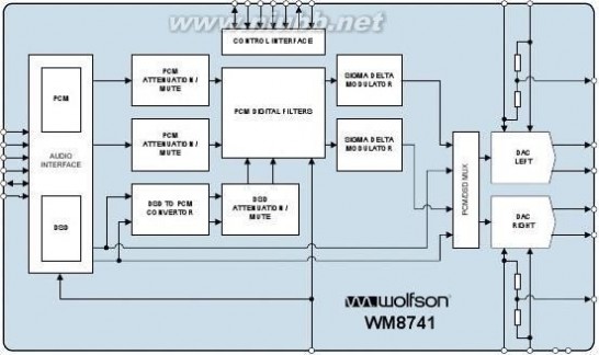
BCLK/DSD64CLK
FSEL/DINRDIN/DINL
LRCLK/DSDL/DSDIN
IWO/DOUTOSR/DSDR
VMIDL
VOUTLP
VOUTLN
VOUTRP
VOUTRN
VMIDR
w
PP Rev 1.3 October 2007
2
8741 WM8741
Product Preview WM8741
TABLE OF CONTENTS
DESCRIPTION.......................................................................................................1
FEATURES.............................................................................................................1
APPLICATIONS.....................................................................................................1
BLOCK DIAGRAM.................................................................................................2
TABLE OF CONTENTS.........................................................................................3
PIN CONFIGURATION...........................................................................................5
ORDERING INFORMATION..................................................................................5
PIN DESCRIPTION (SOFTWARE CONTROL MODE)..........................................6
PIN DESCRIPTION (HARDWARE CONTROL MODE)..........................................8
ABSOLUTE MAXIMUM RATINGS.......................................................................10
THERMAL PERFORMANCE...............................................................................10
RECOMMENDED OPERATING CONDITIONS...................................................11
ELECTRICAL CHARACTERISTICS....................................................................11
MASTER CLOCK TIMING...........................................................................................13
PCM DIGITAL AUDIO INTERFACE TIMINGS.............................................................13
DSD AUDIO INTERFACE TIMINGS............................................................................14
CONTROL INTERFACE TIMING – 3-WIRE MODE....................................................15
CONTROL INTERFACE TIMING – 2-WIRE MODE....................................................16
INTERNAL POWER ON RESET CIRCUIT..................................................................17
DEVICE DESCRIPTION.......................................................................................19
INTRODUCTION.........................................................................................................19
CLOCKING SCHEMES...............................................................................................19
CONTROL INTERFACE..............................................................................................19
SOFTWARE CONTROL INTERFACE.........................................................................20 3-WIRE (SPI COMPATIBLE) SERIAL CONTROL MODE.......................................................................................................20
3-WIRE CONTROL INTERFACE DAISY CHAINING...............................................................................................................20
2-WIRE SERIAL CONTROL MODE...................................................................................................................................22
DIGITAL AUDIO INTERFACE.....................................................................................22 PCM MODE.................................................................................................................................................................22
PCM DIGITAL AUDIO INTERFACE...................................................................................................................................23
LEFT JUSTIFIED MODE..................................................................................................................................................23
RIGHT JUSTIFIED MODE................................................................................................................................................24
2IS MODE....................................................................................................................................................................24
DSP MODE A..............................................................................................................................................................25
DSP MODE B..............................................................................................................................................................25
PCM MODE SAMPLING RATES......................................................................................................................................25
8FS MODE..................................................................................................................................................................26
8FS MODE SAMPLING RATES.......................................................................................................................................27
AUDIO INTERFACE DAISY CHAINING...............................................................................................................................27
DSD MODE.................................................................................................................28 DSD DIRECT...............................................................................................................................................................28
DSD PLUS MODE.........................................................................................................................................................28
DSD DIGITAL AUDIO INTERFACE...................................................................................................................................28
SOFTWARE CONTROL MODE..................................................................................29 DSD AND PCM MODE SWITCHING................................................................................................................................29
PCM DIGITAL AUDIO INTERFACE CONTROL REGISTERS..................................................................................................29
LRCLK POLARITY........................................................................................................................................................30
w
PP Rev 1.3 October 2007 3
8741 WM8741
WM8741 Product Preview
BCLK / DSDCLK64 POLARITY.....................................................................................................................................30 OVERSAMPLING RATE CONTROL...................................................................................................................................30 MCLK/LRCLK RATIO CONTROL (NORMAL PCM MODE).................................................................................................31 8FS MODE..................................................................................................................................................................31 MCLK/LRCLK RATIO CONTROL (8FS MODE)................................................................................................................31 ATTENUATION CONTROL...............................................................................................................................................31 DAC OUTPUT ATTENUATION.........................................................................................................................................32 ATTENUATION CONTROL MODE.....................................................................................................................................32 VOLUME RAMP MODE...................................................................................................................................................33 ANTI-CLIPPING DIGITAL ATTENUATION MODE..................................................................................................................33 DSD PLUS GAIN CONTROL...........................................................................................................................................33 MUTE MODES..............................................................................................................................................................34 ZERO FLAG OUTPUT....................................................................................................................................................35 ZFLAG FORCE HIGH CONTROL....................................................................................................................................35 INFINITE ZERO DETECT.................................................................................................................................................35 DE-EMPHASIS..............................................................................................................................................................36 OUTPUT PHASE REVERSAL...........................................................................................................................................36 DIFFERENTIAL MONO MODE..........................................................................................................................................37 DITHER.......................................................................................................................................................................37 NORMAL PCM MODE DIGITAL FILTER SELECTION...........................................................................................................38 8FS MODE DIGITAL FILTER...........................................................................................................................................38 DSD PLUS FILTER SELECTION......................................................................................................................................38 DSD DIRECT DIGITAL FILTER........................................................................................................................................38 DSD MUTE CONTROL..................................................................................................................................................39 POWER SAVING STANDBY CONTROL.............................................................................................................................39 DSD AND PCM MODE SWITCHING...............................................................................................................................39 AUDIO INPUT FORMAT..................................................................................................................................................39 OVERSAMPLING RATE CONTROL...................................................................................................................................40 MUTE PIN....................................................................................................................................................................40 ZERO FLAG...............................................................................................................................................................41 DE-EMPHASIS CONTROL AND ANTI-CLIPPING MODE........................................................................................................41 DIGITAL FILTER SELECTION...........................................................................................................................................42 DIFFERENTIAL MONO MODE..........................................................................................................................................42 HARDWARE CONTROL MODE..................................................................................39
OVERVIEW OF FUNCTIONS...............................................................................43
REGISTER MAP...................................................................................................44
REGISTER MAP...................................................................................................44
DIGITAL FILTER CHARACTERISTICS...............................................................49
PCM MODE FILTER CHARACTERISTICS.................................................................49
8FS MODE FILTER CHARACTERISTICS...................................................................51
DSD PLUS MODE FILTER CHARACTERISTICS.......................................................52
DSD DIRECT MODE FILTER CHARACTERISTICS...................................................52
PCM MODE FILTER RESPONSES.............................................................................53
8FS MODE FILTER RESPONSES..............................................................................58
DSD PLUS MODE FILTER RESPONSES...................................................................58
DSD DIRECT MODE FILTER RESPONSES...............................................................59
DEEMPHASIS FILTER RESPONSES.........................................................................60
APPLICATIONS INFORMATION.........................................................................61
PACKAGE DIMENSIONS....................................................................................62
IMPORTANT NOTICE..........................................................................................63
ADDRESS:..................................................................................................................63 w
PP Rev 1.3 October 2007 4
8741 WM8741
Product Preview
WM8741
PIN CONFIGURATION


ORDERING INFORMATION
DEVICE
TEMPERATURE
RANGE
PACKAGE 28-lead SSOP (Pb-free) 28-lead SSOP (Pb-free, tape and reel)
MOISTURE SENSITIVITY
LEVEL
MSL 1 MSL 1
PEAK SOLDERING TEMPERATURE
260?C 260?C
° to +85°C ° to +85°C Note:
Reel Quantity = 2,000
w
PP Rev 1.3 October 2007
5
8741 WM8741
WM8741
PIN DESCRIPTION (SOFTWARE CONTROL MODE)
1 2 3 4
LRCLK / DSDL DIN / DINL BCLK / DSD64CLK FSEL / DINR
Digital input Digital input Digital input Digital input Tri-level
PCM MODE Audio interface left/right clock input
Audio interface data input
Audio interface bit clock input Unused
DESCRIPTION 8FS PCM MODE Audio interface left/right clock input
Audio interface left data input
Audio interface bit clock input
Audio interface right data input
Master clock input Differential mono mode selection
0 = normal operation 1 = differential mono mode Digital ground Digital supply
Right analogue positive reference
Right analogue negative reference
Right analogue midrail decoupling pin Right DAC positive output
Right DAC negative output
Analogue ground Analogue supply Left DAC negative output Left DAC positive output Left analogue midrail decoupling pin Left analogue negative reference
Left analogue positive reference Zero flag output Unused
Product Preview
DSD MODES DSD left audio data in Unused
64fs system clock input Unused Unused
Differential mono mode selection
0 = normal operation 1 = differential mono mode Digital ground Digital supply
Right analogue positive reference
Right analogue negative reference
Right analogue midrail decoupling pin Right DAC positive output
Right DAC negative output
Analogue ground Analogue supply Left DAC negative output Left DAC positive output Left analogue midrail decoupling pin Left analogue negative reference
Left analogue positive reference Zero flag output DSD right audio data in
Master clock input Differential mono mode selection Internal pull-0 = normal operation down
1 = differential mono mode Digital ground Digital supply Right analogue positive reference Right analogue negative reference Right analogue midrail decoupling pin Output Right DAC positive output Output Right DAC negative output Output Analogue ground Analogue supply Left DAC negative output Output Left DAC positive output Output Left analogue midrail decoupling pin Output Left analogue negative reference Left analogue positive reference Zero flag output Unused Tri-level 23
IWO / DOUT
Digital input/output
Buffered audio interface data output
w
PP Rev 1.3 October 2007
6
8741 WM8741
Product Preview
24
MODE / LRSEL
Digital input, tri-level
PCM MODE When DIFFHW=0: 0 = hardware mode
1 = 3-wire software mode Z = 2-wire software mode When DIFFHW=1: 0 = left channel mono 1 = right channel mono
DESCRIPTION 8FS PCM MODE When DIFFHW=0: 0 = hardware mode
1 = 3-wire software mode Z = 2-wire software mode When DIFFHW=1: 0 = left channel mono 1 = right channel mono Softmute Control 0 = mute active
1 = normal operation
WM8741
DSD MODES When DIFFHW=0: 0 = hardware mode
1 = 3-wire software mode Z = 2-wire software mode When DIFFHW=1: 0 = left channel mono 1 = right channel mono Softute Control 0 = mute active
1 = normal operation NOTE: In DSD Direct mode this is an analogue mute
25
MUTEB / SDOUT
Digital input or Softmute Control
output: 0 = mute active
Internal pull-up 1 = normal operation
NOTE: In 3-wire mode only, this pin may be used as a buffered control interface data output
Serial control interface data input
Serial control interface clock input
3-wire mode: serial control interface latch 2-wire mode: device address select
Digital input
DEEMPH Tri-level 27
SCLK / DSD
Digital input
Serial control interface data input
Serial control interface clock input
3-wire mode: serial control interface latch 2-wire mode: device address select
Serial control interface data input
Serial control interface clock input
3-wire mode: serial control interface latch 2-wire mode: device address select
Digital input
SADDR /
2IS Notes: 1. 2.
Undefined inputs should be connected to DVDD or DGND
Tri-level pins which require the ‘Z’ state to be selected should be left floating (open)
w
PP Rev 1.3 October 2007
7
8741 WM8741
WM8741
PIN DESCRIPTION (HARDWARE CONTROL MODE)
PCM MODE
1 2 3 4
LRCLK / DSDL DIN / DINL BCLK / DSD64CLK FSEL / DINR
Digital input Digital input Digital input Digital input Tri-level
Audio interface left/right clock input Audio interface data input Audio interface bit clock input Selects between one of three digital filters – see Table 48
DESCRIPTION
Product Preview
DSD DIRECT MODE
DSD left audio data in Unused
64fs system clock input Unused Unused
Differential mono mode selection 0 = normal operation
1 = differential mono mode Digital ground Digital supply
Right analogue positive reference Right analogue negative reference Right analogue midrail decoupling pin Right DAC positive output Right DAC negative output Analogue ground Analogue supply Left DAC negative output Left DAC positive output
Left analogue midrail decoupling pin Left analogue negative reference Left analogue positive reference Zero flag output DSD right audio data in
Master clock input Differential mono mode selection 0 = normal operation Internal pull-down 1 = differential mono mode Digital ground Digital supply Right analogue positive reference Right analogue negative reference Right analogue midrail decoupling pin Output Right DAC positive output Output Right DAC negative output Output Analogue ground Analogue supply Left DAC negative output Output Left DAC positive output Output
Left analogue midrail decoupling pin Output Left analogue negative reference Left analogue positive reference Zero flag output Controls internal oversampling rate: 0 = low rate Tri-level
Z = medium rate 1 = high rate 23
IWO / DOUT
Digital input/output
Controls audio interface wordlength – see Table 44
Unused
w
PP Rev 1.3 October 2007
8
8741 WM8741
Product Preview
PCM MODE
24
MODE / LRSEL
Digital input, tri-level
When DIFFHW=0: 0 = hardware mode
1 = 3-wire software mode Z = 2-wire software mode When DIFFHW=1: 0 = left channel mono 1 = right channel mono
DESCRIPTION
WM8741
DSD DIRECT MODE
When DIFFHW=0: 0 = hardware mode
1 = 3-wire software mode Z = 2-wire software mode When DIFFHW=1: 0 = left channel mono 1 = right channel mono Analogue Mute Control 0 = mute active
1 = normal operation Unused
25
MUTEB / SDOUT
Digital input or Softmute Control
output: 0 = mute active
Internal pull-up 1 = normal operation
De-emphasis Control 0 = normal operation 1 = de-emphasis applied
Z = anti-clipping digital filter mode HW Mode Select: 0 = PCM
1 = DSD Direct
Controls audio interface format – see Table 44
Digital input
DEEMPH Tri-level
27
SCLK / DSD
Digital input
HW Mode Select: 0 = PCM
1 = DSD Direct Unused
Digital input
SADDR /
2IS Notes: 1. 2.
Undefined inputs should be connected to DVDD or DGND
Tri-level pins who require the ‘Z’ state to be selected should be left floating (open)
w
PP Rev 1.3 October 2007
9
8741 WM8741
WM8741
Product Preview
ABSOLUTE MAXIMUM RATINGS
Absolute Maximum Ratings are stress ratings only. Permanent damage to the device may be caused by continuously operating at or beyond these limits. Device functional operating limits and guaranteed performance specifications are given under Electrical

Characteristics at the test conditions specified.
ESD Sensitive Device. This device is manufactured on a CMOS process. It is therefore generically
susceptible to damage from excessive static voltages. Proper ESD precautions must be taken during handling and storage of this device.
Wolfson Microelectronics tests its package types according to IPC/JEDEC J-STD-020B for Moisture Sensitivity to determine acceptable storage conditions prior to surface mount assembly. These levels are:
MSL1 = unlimited floor life at <30°C / 85% Relative Humidity. Not normally stored in moisture barrier bag. MSL2 = out of bag storage for 1 year at <30°C / 60% Relative Humidity. Supplied in moisture barrier bag. MSL3 = out of bag storage for 168 hours at <30°C / 60% Relative Humidity. Supplied in moisture barrier bag. The Moisture Sensitivity Level for each package type is specified in Ordering Information. CONDITION
Digital supply voltage, DVDD Analogue supply voltage, AVDD Voltage range digital inputs Voltage range analogue inputs Master Clock Frequency Operating temperature range, TA Storage temperature
Ambient temperature (supplies applied)
Pb free package body temperature (soldering 10 seconds) Pb free package body temperature (soldering 2 minutes) Notes:
1. Analogue and digital grounds must always be within 0.3V of each other.
DGND - 0.3V AGND - 0.3V
DVDD + 0.3V AVDD + 0.3V
THERMAL PERFORMANCE
TEST Thermal resistance –
junction to case Thermal resistance – junction to ambient
θJC°C/W θJA°C/W
w
PP Rev 1.3 October 2007
10
8741 WM8741
Product Preview
WM8741
RECOMMENDED OPERATING CONDITIONS
TEST Digital supply range Analogue supply range Ground
Difference DGND to AGND Analogue operating current Digital operating current Analogue standby current Digital standby current
IAVDDIDVDDAVDD DVDD IAVDD (Standby)Clocks stopped IDVDD (Standby) Clocks stopped
ELECTRICAL CHARACTERISTICS
TEST CONDITIONS
AVDD = 5V, DVDD = 3.3V, AGND, DGND = 0V, TA = +25C, 1kHz test signal, fs = 48kHz, MCLK = 256fs unless otherwise stated.
TEST Digital Logic Levels Input LOW level Input HIGH level Output LOW level Output HIGH level
DSD Input Characteristics Full-scale modulation depth DAC Performance Signal to Noise Ratio (Note 1)
SNR
o
VIL VIH VOL VOH
IOL = 2mA IOH = 2mA
=DSD Direct or DSD Plus Mode =
A-weighted mono @ fs = 48kHz A-weighted stereo @ fs = 48kHz A-weighted stereo @ fs = 96kHz A-weighted stereo @ fs = 192kHz Non-weighted stereo
@ fs = 48kHz
0.7 x DVDD
0.9 x DVDD
-2.9 71.6
0.1 x DVDD
V V V
%
-100 -100 -100 -100
dB dB dB dB
Dynamic Range
(Note 2)
Total Harmonic Distortion (Note 2)
-60dB full scale input THD
Mono 0dB @ fs = 48kHz Stereo 0dB @ fs = 48kHz Stereo 0dB @ fs = 96kHz Stereo 0dB @ fs = 192kHz
Channel Separation Channel Level Matching Channel Phase Deviation Power Supply Rejection Ratio
DegreePSRR
100mVpp at 1kHz 20Hz to 20kHz 100mVpp
-80 -67
dB dB
w
PP Rev 1.3 October 2007
11
8741 WM8741
WM8741
TEST CONDITIONS
Product Preview
AVDD = 5V, DVDD = 3.3V, AGND, DGND = 0V, TA = +25oC, 1kHz test signal, fs = 48kHz, MCLK = 256fs unless otherwise stated.
TEST Internal Analogue Filter Bandwidth
Passband edge response Analogue Output Levels PCM full scale differential output level
DSD Direct full scale differential output level DSD Plus full scale differential output level Minimum resistance load Maximum capacitance load Output DC level Reference Levels Potential divider resistance Voltage at VMIDL/VMIDR Notes:
1. Ratio of output level with 1kHz full scale input, to the output level with all zeros into the digital input, measured ‘A’
weighted over a 20Hz to 20kHz bandwidth. 2.
All performance measurements done with 20kHz low pass filter. Failure to use such a filter will result in higher THD and lower SNR and Dynamic Range readings than are found in the Electrical Characteristics. The low pass filter removes out of band noise; although it is not audible it may affect dynamic specification values.
10k? load, 0dBFS input 10k? load, 0dBFS input 10k? load, 0dBFS input
To midrail or AC coupled
2 1.34 1.4 2
VRMS VRMS VRMS k?
AVDD to VMIDL/VMIDR and VMIDL/VMIDR to AGND
k?
w
PP Rev 1.3 October 2007
12
8741 WM8741
Product Preview WM8741
MASTER CLOCK TIMING
Figure 1 Master Clock Timing Requirements
Test Conditions
oAVDD = 5V, DVDD = 3.3V, AGND = 0V, DGND = 0V, TA = +25C Master Clock Timing Information
MCLK Master clock pulse width high MCLK Master clock pulse width low
MCLK Master clock cycle time
MCLK Duty cycle
Table 1 MCLK Timing Requirements tMCLKH tMCLKL tMCLKY

PCM DIGITAL AUDIO INTERFACE TIMINGS
Figure 2 Digital Audio Data Timing
Test Conditions
AVDD = 5V, DVDD = 3.3V, AGND = 0V, DGND = 0V, TA = +25oC, fs = 48kHz, MCLK = 256fs unless otherwise stated. TEST Audio Data Input Timing Information
BCLK cycle time
BCLK pulse width high
BCLK pulse width low
LRCLK set-up time to BCLK
rising edge
LRCLK hold time from
BCLK rising edge
DIN set-up time to BCLK
rising edge
DIN hold time from BCLK
rising edge tBCY tBCH tBCL tLRSU tLRH tDS tDH Table 2 Digital Audio Interface Timing Requirements
w
PP Rev 1.3 October 2007 13

8741 WM8741
WM8741

Product Preview
DSD AUDIO INTERFACE TIMINGS
Figure 3 DSD Audio Timing - Normal Mode

Figure 4 DSD Audio Timing - Phase Modulated Mode
Test Conditions
DVDD = 3.3V, GND = 0V, TA = +25oC, fs = 44.1kHz, DSDCLK64 = 64fs unless otherwise stated. TEST Audio Data Input Timing Information
DSDCLK64 cycle time
DSDCLK64 pulse width high
DSDCLK64 pulse width low
DSD[0:1] set-up time to
DSDCLK64 rising edge
DSD[0:1] hold time from
DSDCLK64 rising edge
Difference in edge timing of
DSD[0:1] to DSDCLK64 t64CY t64H t64L tDSN tDHN tDC Table 3 DSD Audio Interface Timing Requirements
w
PP Rev 1.3 October 2007 14
8741 WM8741
Product Preview WM8741
CONTROL INTERFACE TIMING – 3-WIRE MODE
Figure 5 Control Interface Timing - 3-Wire Serial Control Mode
Test Conditions
oDVDD = 3.3V, GND = 0V, TA = +25C, fs = 48kHz, MCLK = 256fs unless otherwise stated. SCLK rising edge to LATCH
rising edge
SCLK pulse cycle time
SCLK pulse width low
SCLK pulse width high
SDIN to SCLK set-up time
SCLK to SDIN hold time
LATCH pulse width low
LATCH pulse width high
LATCH rising to SCLK rising tSCStSCY tSCL tSCHtDSUtDHOtCSLtCSHtCSSTable 4 Control Interface Timing – 3-Wire Serial Control Mode
w
PP Rev 1.3 October 2007 15


8741 WM8741
WM8741
CONTROL INTERFACE TIMING – 2-WIRE MODE
Product Preview
Figure 6 Control Interface Timing - 2-Wire Serial Control Mode
Test Conditions
DVDD = 3.3V, DGND = 0V, TA = +25oC, Slave Mode, fs = 48kHz, MCLK = 256fs unless otherwise stated. SCLK Frequency SCLK Low Pulse-Width SCLK High Pulse-Width Hold Time (Start Condition) Setup Time (Start Condition) Data Setup Time SDIN, SCLK Rise Time SDIN, SCLK Fall Time Setup Time (Stop Condition) Data Hold Time
Max Pulse width of spikes that will be suppressed
Table 5 Control Interface Timing – 2-wire Serial Control Mode
tSCLtSCHtHOLtCSEtDSUtRIStFALtCSStDHOtPSw
PP Rev 1.3 October 2007
16


8741 WM8741
Product Preview
WM8741
The WM8741 includes two internal Power On Reset (POR) circuits which are used to reset the digital logic into a default state after power up and to allow the analogue circuits to power-up silently. The digital POR circuit is powered from DVDD. This circuit monitors DVDD and asserts the internal digital reset if DVDD are below the minimum DVDD threshold which will allow the digital logic to function.
The analogue POR circuit is powered from AVDD. The circuit monitors AVDD, tri-stating the DAC outputs and isolating the internal reference resistor strings from AVDDL and AVDDR until there is

sufficient AVDD voltage to allow the analogue DAC stages to function correctly.
INTERNAL POWER ON RESET CIRCUIT
Figure 7 AVDD Power up Sequence
Test Conditions
AVDD = 5V, AGND = 0V, TA = +25oC, TA_max = +125oC, TA_min = -25oC, AVDDmax = 5.5V, AVDDmin = 4.5V
TEST Power Supply Input Timing Information AVDD level to POR rising edge (AVDD rising) AVDD level to POR falling edge (AVDD falling)
Table 6 Analogue POR Timing
Vpor_hi Vpor_lo
Measured from AGND Measured from AGND
2.00 1.84
V V
w
PP Rev 1.3 October 2007
17
8741 WM8741
WM8741
Product Preview
Figure 8 DVDD Power up Sequence
Test Conditions
DVDD = 3.3V, DGND = 0V, TA = +25oC, TA_max = +125oC, TA_min = -25oC, DVDDmax = 3.6V, DVDDmin = 3.0V
TEST Power Supply Input Timing Information DVDD level to POR rising edge (DVDD rising) DVDD level to POR falling edge (DVDD falling) Table 7 Digital POR Timing
In a real application the designer is unlikely to have control of the relative power up sequence of AVDD and DVDD. The POR circuit ensures a reasonable delay between applying power to the device and Device Ready.
Figure 7 and Figure 8 show typical power up scenarios in a real system. DVDD must be established before the device can be written to. Any writes to the device before device ready will be ignored. Note: DVDD must be established before the MCLK is started. This will ensure all synchronisation circuitry within the device is fully initialised and ready.
AVDD must be established before the device will output any signal. Whilst the device will output signal as soon as the Internal Analogue PORB indicates device ready, normal operation is not possible until the VMID pin has reached the midrail voltage.
Vpor_hi Vpor_lo
Measured from DGND Measured from DGND
1.86 1.83
V V
w
PP Rev 1.3 October 2007
18

8741 WM8741
Product Preview WM8741 DEVICE DESCRIPTION
INTRODUCTION
The WM8741 is an ultra high performance DAC designed for digital audio applications. Its range of
features makes it ideally suited for use in professional recording environments, CD/DVD players, AV
receivers and other high-end consumer audio equipment.
The WM8741 is a complete differential stereo audio digital-to-analogue converter. The system
includes a dithered digital interpolation filter, fine resolution volume control and digital de-emphasis,
followed by a multi-bit sigma delta modulator and switched capacitor multi-bit stage with differential
voltage outputs. The device supports both PCM and DSD digital audio input formats.
The WM8741 includes a configurable digital audio interface support for a 3-wire and 2-wire serial
control interface, and a hardware control interface. The software control interface may be
asynchronous to the audio data interface; in which case control data will be re-synchronised to the
audio processing internally. It is fully compatible with, and an ideal partner for, a range of industry
standard microprocessors, controllers and DSPs.
Uniquely, the WM8741 has a large range of high performance low latency advanced digital filters.
The full range of filters is selectable in software mode, and a limited range of filters are available
under hardware control. The filters allow users the flexibility to choose characteristics to match their
group delay, phase and latency requirements.
Operation using a master clock of 128fs, 192fs, 256fs, 384fs, 512fs or 768fs is supported. Sample
rates (fs) from 32kHz to 192kHz are allowed, provided the appropriate master clock is input (see
Table 1 for details).
In normal PCM mode, the audio data interface supports right justified, left justified and IS interface
formats along with a highly flexible DSP serial port interface.
There are two DSD modes. In DSD Direct mode, the datastream is subjected to the minimum
possible processing steps between input and output. In DSD Plus mode, the datastream is
converted to PCM and filtered to allow reduction of out of band components. This step also provides
additional benefits in allowing access to other PCM features such as volume control and advanced
digital filtering.
The device is packaged in a small 28-lead SSOP. 2
CLOCKING SCHEMES
In a typical digital audio system there is only one central clock source producing a reference clock to

which all audio data processing is synchronised. This clock is often referred to as the audio system’s
Master Clock. The external master system clock can be applied directly through the MCLK input pin
with no software configuration necessary for sample rate selection.
MCLK is used to derive clocks for the DAC path in PCM mode. The DAC path consists of DAC
sampling clock, DAC digital filter clock and DAC digital audio interface timing. In a system where
there are a number of possible sources for the reference clock it is recommended that the clock
source with the lowest jitter be used to optimise the performance of the DAC.
CONTROL INTERFACE
The WM8741 supports 2-wire and 3-wire serial control, and hardware control. Selection of control
mode is made by controlling the state of the MODE pin. 24 MODE/
LRSEL DESCRIPTION 0 = Hardware control mode 1 = 3-wire serial control mode
Z = 2-wire serial control mode
Table 8 Control Mode Configuration
w
PP Rev 1.3 October 2007 19
8741 WM8741
WM8741
SOFTWARE CONTROL INTERFACE
Product Preview
The software control interface may be operated using a 2-wire or 3-wire (SPI-compatible) serial interface. When operating under serial control, hardware configuration pins are ignored.
Note: DIFFHW will override all other pins, forcing the device into hardware control mode and differential mode mode.
3-WIRE (SPI COMPATIBLE) SERIAL CONTROL MODE
Every rising edge of SCLK clocks in one bit of data on SDIN. A rising edge on CSB latches a

complete control word consisting of 16 bits. The 3-wire interface protocol is shown in Figure 9.
Figure 9 3-wire Serial Interface Protocol Notes: 1. 2. 3.
A[6:0] are Control Address Bits D[7:0] are Control Data Bits D[8] is always set to zero
3-WIRE CONTROL INTERFACE DAISY CHAINING
In daisy chaining mode, SDOUT (pin 25) outputs control data sampled on SDIN with a delay of 16 SCLK cycles. This data signal can be used to control another WM8741 in a daisy chain circuit as shown in Figure 10.
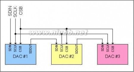
Figure 10 Control Interface Daisy Chaining Setup
To configure devices into daisy chain mode the CSB signal should be driven low while there is a register write to set register bit SDOUT=1. CSB should then be driven high, this sets the first device in daisy chain mode. CSB should then be driven low again while register bit SDOUT is set high. Setting CSB high again will cause the first register write to be output to the second device from the SDOUT pin, this sets the second device into daisy chain mode. This method must be repeated for the number of devices in the chain until they are all set into daisy chain mode. Figure 11 shows the protocol for configuring the first two devices in the daisy chain.
w
PP Rev 1.3 October 2007
20
8741 WM8741
Product Preview WM8741
Figure 11 Initial Setup of Two WM8741 Devices into Control Interface Daisy Chain Mode
To write to a single device in the chain a complete sequence needs to be written to all the devices.
Devices that do not require a register change must also be written to. The user can choose to write
either the same data as the previous write, or write all 1s for the register address and data. All 1s will
result in writing to a non-existent register, address 7Fh, preserving the current register settings.
Figure 12 shows an example of how to access three WM8741 devices (the devices have all


previously been configured in daisy chain mode):
Figure 12 Daisy Chain Control Interface Example for Three WM8741 Devices
To ensure that only valid data is written to the devices in daisy chain mode, a pull up resistor is used
in SDOUT. When connected to the SDIN pin of the next device in the chain, this results in all ones
being written to the control interface of that device until the correct daisy chain data is written and
latched.
Serial daisy chaining is available only when using 3-wire serial control mode. It is not available in 2-
wire serial control mode or hardware control mode. REGISTER ADDRESS
R8
Mode Control 2
08h BIT LABEL DEFAULT 0 DESCRIPTION 3 wire Serial Interface Daisy Chaining 0 = No Output
1 = Output on pin 25. Table 9 Control Interface Daisy Chaining Selection
w
PP Rev 1.3 October 2007 21


8741 WM8741
WM8741 2-WIRE SERIAL CONTROL MODE Product Preview
The WM8741 supports software control via a 2-wire serial bus. Many devices can be controlled by the same bus, and each device has a unique 7-bit address (this is not the same as the 7-bit address of each register in the WM8741).
The WM8741 operates as a slave device on the 2-wire control bus. The controller indicates the start of data transfer with a high to low transition on SDIN while SCLK remains high. This indicates that a device address and data will follow. All devices on the 2-wire bus respond to the start condition and shift in the next eight bits on SDIN (7-bit address + Read/Write bit, MSB first). If the device address received matches the address of the WM8741 and the R/W bit is ‘0’, indicating a write, then the WM8741 responds by pulling SDIN low on the next clock pulse (ACK). If the address is not recognised or the R/W bit is ‘1’, the WM8741 returns to the idle condition and wait for a new start condition and valid address.
Once the WM8741 has acknowledged a correct address, the controller sends the first byte of control data (B15 to B8, i.e. the WM8741 register address plus the first bit of register data). The WM8741 then acknowledges the first data byte by pulling SDIN low for one clock pulse. The controller then sends the second byte of control data (B7 to B0, i.e. the remaining 8 bits of register data), and the WM8741 acknowledges again by pulling SDIN low.
The transfer of data is complete when there is a low to high transition on SDIN while SCLK is high. After receiving a complete address and data sequence the WM8741 returns to the idle state and waits for another start condition. If a start or stop condition is detected out of sequence at any point


during data transfer (i.e. SDIN changes while SCLK is high), the device reverts to the idle condition.
Figure 13 2-wire Serial Control Interface
The WM8741 device address can be configured between two options. This is selected by the SADDR pin. 28 CSB/
SADDR/I2S DESCRIPTION 0 = 2-wire address 0011010 1 = 2-wire address 0011011
Table 10 2-wire Serial Control Mode Address Selection
DIGITAL AUDIO INTERFACE
PCM MODE
There are a number of valid PCM data input modes. Two channel and one channel differential mono modes can be selected by serial or hardware control. It is also possible to bypass the WM8741 digital filters and apply a signal at a rate 8fs (where fs is the sampling rate) directly to the switched capacitor stage..
w
PP Rev 1.3 October 2007 22
8741 WM8741
Product Preview WM8741
PCM DIGITAL AUDIO INTERFACE
Audio data is applied to the DAC system via the Digital Audio Interface. Five popular interface
formats are supported:
? Left Justified mode
? Right Justified mode
?
?
? I2S mode DSP mode A DSP mode B
All five formats require the MSB to be transmitted first, and support word lengths of 16, 20, 24 and 32
bits, with the exception that 32 bit data is not supported in right justified mode. DIN and LRCLK may
be configured to be sampled on the rising or falling edge of BCLK by adjusting register bits LRP and
BCP.
In left justified, right justified and I2S audio interface modes, the digital audio interface receives data
on the DIN input pin. Stereo audio data is time multiplexed on DIN, with LRCLK indicating whether
the left or right channel is present. LRCLK is also used as a timing reference to indicate the
beginning or end of the data words.
The minimum number of BCLK periods per LRCLK period is two times the selected word length.
LRCLK must be high for a period equal to the minimum number of BCLK periods, and low for a
minimum of the same period. Any mark-to-space ratio on LRCLK is acceptable provided the above
requirements are met.
The WM8741 will automatically detect when data with a LRCLK period of exactly 32 BCLKs is
received, and select 16-bit mode. This overrides any previously programmed word length. The
operating word length will revert to a programmed value only if a LRCLK period other than 32 BCLKs
is detected.
In DSP mode A or DSP mode B, the data is time multiplexed onto DIN. LRCLK is used as a frame
sync signal to identify the MSB of the first word. The minimum number of BCLKs per LRCLK period
is two times the selected word length. Any mark to space ratio is acceptable on LRCLK provided the
rising edge is correctly positioned.
LEFT JUSTIFIED MODE
In left justified mode, the MSB is sampled on the first rising edge of BCLK following a LRCLK


transition. LRCLK is high during the left data word and low during the right data word.
Figure 14 Left Justified Mode Timing Diagram
w
PP Rev 1.3 October 2007 23
8741 WM8741
WM8741 RIGHT JUSTIFIED MODE Product Preview
In right justified mode, the LSB is sampled on the rising edge of BCLK preceding a LRCLK transition.


LRCLK is high during the left data word and low during the right data word.
Figure 15 Right Justified Mode Timing Diagram
IS MODE
In IS mode, the MSB is sampled on the second rising edge of BCLK following a LRCLK transition.


LRCLK is low during the left data word and high during the right data word. 22
Figure 16 IS Mode Timing Diagram 2
w
PP Rev 1.3 October 2007 24
8741 WM8741
Product Preview WM8741
DSP MODE A
In DSP mode A, the first bit is sampled on the BCLK rising edge following the one that detects a low
to high transition on LRCLK. No BCLK edges are allowed between the data words. The word order

is DIN left, DIN right.
Figure 17 DSP Mode A Timing Diagram
DSP MODE B
In DSP mode B, the first bit is sampled on the BCLK rising edge, which detects a low to high
transition on LRCLK. No BCLK edges are allowed between the data words. The word order is DIN

left, DIN right.
Figure 18 DSP Mode B Timing Diagram
PCM MODE SAMPLING RATES
The WM8741 supports master clock rates of 128fs to 768fs, where fs is the audio sampling
frequency (LRCLK), typically 32kHz, 44.1kHz, 48kHz, 88.2kHz, 96kHz, 176.4kHz or 192kHz.
The WM8741 has a master clock detection circuit that automatically determines the relationship
between the master clock frequency and the sampling rate. The master clock should be
synchronised with LRCLK, although the WM8741 is tolerant of phase differences or jitter on this
clock.
w
PP Rev 1.3 October 2007 25
8741 WM8741
WM8741
SAMPLING RATE (LRCLK)
MASTER CLOCK (MCLK) FREQUENCY (MHZ)
Product Preview
Unavailable Unavailable Unavailable
176.4kHz 192kHz
22.5792 24.576
33.8688 36.864
Table 11 Typical Relationships Between Master Clock Frequency and Sampling Rate in normal
PCM mode
8FS MODE
Operation in 8FS mode requires that audio data for left and right channels is input separately on two pins. DINR (pin 4) is the input for right channel data and DINL (pin 2) is the input for left channel data. Hardware control of the device is not available.
The data can be input in two formats (left or right justified), selectable by register FMT[1:0], and two word lengths (20 or 24 bit), selectable by register IWL[1:0]. In both modes the data is clocked into the WM8741 MSB first.
For left justified data the word start is identified by the falling edge of LRCLK. The data is clocked in on the next 20/24 BCLK rising edges. This format is compatible with industry-standard DSPs and

decoders such as the PMD100.
Figure 19 8FS Mode Left Justified Timing Requirements
For right justified mode, the data is justified to the rising edge of LRCLK and the data is clocked in on the preceding 20/24 BCLK rising edges before the LRCLK rising edge. This format is compatible

with industry standard DSPs and decoders such as the DF1704 or SM5842.
Figure 20 8FS Mode Right Justified Timing Requirements
w
PP Rev 1.3 October 2007
26
8741 WM8741
Product Preview
In both modes the polarity of LRCLK can be switched using register bit LRP.
WM8741
8FS MODE SAMPLING RATES
Since the data rate in 8FS mode is much faster than in standard PCM mode, there are restrictions on the MCLK rate that can be used. Specifically, only 512fs and 768fs modes are permitted restricting the sample rate to a maximum of 8x48kHz. The master clock should be synchronised with LRCLK, although the WM8741 is tolerant of phase differences or jitter on this clock.
Unlike in normal PCM mode, the master clock detection circuit does not operate in 8FS mode. The rate must be manually programmed using the control interface. SAMPLING RATE
fs
LRCLK FREQUENCY
(kHz)
MASTER CLOCK (MCLK) FREQUENCY (MHz)


Table 12 Typical Relationships Between Master Clock Frequency and Sampling Rate in 8FS Mode

AUDIO INTERFACE DAISY CHAINING
In daisy chain mode the DOUT pin outputs the audio data received on the DIN pin but delayed by two times the input word length. When this output is connected to the DIN pin of the next device in the

chain, each WM8741 device will simultaneously sample different channel data in the same LRCLK period. Daisy chaining is only available in DSP audio interface mode and is limited by a maximum BCLK frequency of 24.576MHz. REGISTER ADDRESS
R8
Mode Control 2

08h
BIT
LABEL
DEFAULT


DESCRIPTION

Daisy Chaining Multiple devices – multichannel off one PCM feed.

0 = No Output


1 = Output on pin 23.
Table 13 Daisy Chaining Audio Data Output Control


The following diagram illustrates timing for a daisy chain with 2 WM8741 devices.
Figure 21 Audio Interface Daisy Chaining Timing
w
PP Rev 1.3 October 2007
27
8741 WM8741
WM8741 DSD MODE Product Preview
The WM8741 supports DSD input bitstreams at 64x the oversampling rate. The data is supplied at a rate of 64 bits per normal word clock. In DSD, no word clock is provided.
The WM8741 supports two channels of bitstream or DSD audio. Data bitstreams and the 64fs clock are supplied to pins 1, 22 and 3 respectively. The MODESEL[1:0] register bits control whether the device operates in DSD direct, DSD plus or PCM modes.
DSD DIRECT
In DSD Direct mode the internal digital filters are bypassed, the input bitstream data is subjected to the minimal possible processing and is applied directly to the switched capacitor stage of the DAC system. Using this mode provides the purest possible representation of a DSD stream.
It is normally desirable to use an external analogue post-DAC analogue filter to combine the differential outputs of the DAC and remove high frequency energy from the output. This is particularly important in the case of DSD operation due to the presence of high frequency energy which is a result of the aggressive high order noise shaping used in the creation of the modulated DSD datastream.
DSD PLUS MODE
In DSD Plus mode the DSD data can be filtered in a similar manner to the data in the PCM path. The DSD Plus filters are selected using register bits DSDFILT[1:0]. DSD Plus mode is not available under hardware control.
Although DSD Plus mode requires that the bitstream is more heavily processed than DSD Direct, the advantage is that DSD Plus mode reduces the high frequency energy which is a result of the aggressive high order noise shaping used in the creation of the modulated DSD datastream. This means that a less aggressive, lower order, analogue filter can be used at the output. Furthermore the slew-rate requirements of the op-amps can be relaxed compared to DSD direct mode, due to the reduction in high frequency energy.
DSD DIGITAL AUDIO INTERFACE
DSD audio data is input to the WM8741 via the DSD digital audio interface. Two interface formats are supported:
? Uni-phase
? Bi-phase
To use this interface apply left data on input pin 1 (LRCLK/DSDL) and pin 22 (OSR/DSDR). A DSD

clock is also required, running at 64FS, and should be applied to pin 3 (BCLK/DSD64CLK).
Figure 22 Uni-phase DSD Mode Timing Diagram
w
PP Rev 1.3 October 2007 28
8741 WM8741
Product Preview
WM8741
Figure 23 Bi-phase DSD Mode Timing Diagram
SOFTWARE CONTROL MODE
Software control allows access to all features of the WM8741. Selection of control mode is achieved by configuring the state of MODE/LRSEL (pin 24):
24
MODE/ LRSEL
DESCRIPTION
0 = Hardware control mode 1 = 3-wire serial control mode Z = 2-wire serial control mode
Table 14 Control Mode Configuration
DSD AND PCM MODE SWITCHING
The audio interface mode can be switched between DSD and PCM by writing MODESEL[1:0] in R7. It is recommended that the chip is forced into a MUTE state before dynamically switching modes. REGISTER ADDRESS
R7
Mode Control 1
07h
BIT
LABEL
DEFAULT
00
DESCRIPTION
DSD/PCM mode select : 00 = PCM mode
01 = Direct DSD Operation 10 = DSD plus mode 11 = Unused
Table 15 PCM/DSD Software Mode Selection
PCM DIGITAL AUDIO INTERFACE CONTROL REGISTERS
The PCM digital audio input format is configured by register bits FMT [1:0] and IWL[1:0]: REGISTER ADDRESS
R5
Format Control
05h
BIT
LABEL
DEFAULT
10
DESCRIPTION
Audio interface input word length select
00 = 16-bit 01 = 20-bit 10 = 24-bit 11 = 32-bit
Audio interface input format select 00 = Right justified 01 = Left justified
2
10 = IS 11 = DSP
10
Table 16 Interface Format Controls Note: 1.
In all modes, the data is signed 2's complement. The WM8741 digital filters always input 24-bit data. If the interface is programmed into 32 bits, dither is applied according to Table 37 before truncation to the internal wordlength.
PP Rev 1.3 October 2007
29

w
8741 WM8741
WM8741
LRCLK POLARITY
Product Preview
In left justified, right justified or I2S modes, the LRP register bit controls the polarity of LRCLK. If this bit is set high, the expected polarity of LRCLK will be the opposite of that shown in Figure 14, Figure 15 and Figure 16. If this feature is used as a means of swapping the left and right channels, a 1 sample phase difference will be introduced. REGISTER ADDRESS
R5
Format Control
05h
BIT 4
LABEL LRP
DEFAULT
DESCRIPTION
LRCLK polarity select: 0 = normal LRCLK polarity 1 = inverted LRCLK polarity
Table 17 LRCLK Polarity Control
In DSP modes, the LRP register bit is used to select between DSP mode A and B (see Figure 17 and Figure 18).
REGISTER ADDRESS
R5
Format Control
05h
BIT
LABEL
DEFAULT
DESCRIPTION
0 DSP format select:
0 = DSP mode A 1 = DSP mode B
Table 18 DSP Format Control
BCLK / DSDCLK64 POLARITY
In PCM mode, LRCLK and DIN are sampled on the rising edge of BCLK by default, and should ideally change on the falling edge. Data sources which change LRCLK and DIN on the rising edge of BCLK can be supported by setting the BCP register bit. Setting BCP to 1 inverts the polarity of BCLK to the inverse of that shown in Figure 14, Figure 15, Figure 16, Figure 17 and Figure 18. In DSD mode, DSDL and DSDR inputs are sampled a fixed delay after a falling 64fs clock edge. When BCP is set in DSD mode, DSDL and DSDR are sampled a fixed delay after a rising 64fs clock edge.
REGISTER ADDRESS
R5
Format Control
05h
BIT 5
LABEL BCP
DEFAULT
DESCRIPTION
BCLK / DSD64CLK polarity select: 0 = normal polarity 1 = inverted polarity
Table 19 BCLK Polarity Control
OVERSAMPLING RATE CONTROL
The user has control of the oversampling ratio of the WM8741, and can set to the device to operate in low, medium or high rate modes. For correct operation of the digital filtering and other processing on the WM8741, the user must ensure the correct value of OSR[1:0] is set at all times. REGISTER ADDRESS
R7
Mode Control 1
07h
BIT
LABEL
DEFAULT
00
DESCRIPTION
Oversampling Rate Selection 00 = Low rate (32/44.1/48kHz) 01 = Medium rate (96kHz) 10 = High rate (192kHz) 11 = Unused
Table 20 Oversampling Rate Control
w
PP Rev 1.3 October 2007
30
8741 WM8741
Product Preview
WM8741
MCLK/LRCLK RATIO CONTROL (NORMAL PCM MODE)
The ratio of MCLK/LRCLK can be programmed directly or auto-detected. REGISTER ADDRESS
R7
Mode Control 1
07h
BIT
LABEL
DEFAULT 000
DESCRIPTION
MCLK to LRCLK sampling rate ratio control (Normal PCM Mode): 000 = auto detect sample rate 001 = 128fs 010 = 192fs 011 = 256fs 100 = 384fs 101 = 512fs 110 = 768fs 111 = reserved
Table 21 MCLK/LRCLK Ratio Control (Normal PCM Mode)
8FS MODE
8FS Mode allows the use of custom digital filters by bypassing the WM8741 internal digital filters. When MODE8X is set, the PCM data input to the WM8741 is applied only to the digital volume control and then the analogue section of the DAC system, bypassing the digital filters. REGISTER ADDRESS
R7
Format Control
07h Table 22 8FS Mode Control
BIT
LABEL
DEFAULT
DESCRIPTION
8FS mode select: 0 = Normal operation
1 = 8FS mode (digital filters bypassed)
MCLK/LRCLK RATIO CONTROL (8FS MODE)
In 8FS mode the choice of clock ratios and sampling rates is limited – see Table 12 for details. Autodetect of MCLK/LRCLK ratio is not available in 8FS mode and must be set manually by the user for correct operation. REGISTER ADDRESS
R7
Mode Control 1
07h
BIT
LABEL
DEFAULT 000
DESCRIPTION
MCLK to LRCLK sampling rate ratio control (8FS Mode): 000 = reserved 001 = 512fs 010 = 768fs
011 to 111 = reserved
Table 23 MCLK/LRCLK Ratio Control (8FS Mode)
ATTENUATION CONTROL
Each DAC channel can be attenuated digitally before being applied to the digital filter. Attenuation is set to 0dB by default but can be set between 0dB and -127.5dB in 0.125dB steps using the ten attenuation control bits LAT[4:0], LAT[9:5], RAT[4:0] and RAT[9:5].
All attenuation registers are double latched allowing new values to be pre-latched to both channels before being updated synchronously. Setting the UPDATE bit on any attenuation write will cause all pre-latched values to be immediately applied to the DAC channels.
w
PP Rev 1.3 October 2007
31
8741 WM8741
WM8741 REGISTER
ADDRESS
R0
DACLLSB
Attenuation
00h DESCRIPTION Product Preview 00 (0dB) LSBs of attenuation data for left channel in 0.125dB steps. See Table 25 for details. 5 Attenuation data load control for left channel. 0 = Store LAT[4:0] value but don’t update
1 = Store LAT[4:0] and update attenuation on registers 0-3
LAT[9:5] 00 (0dB) MSBs of attenuation data for left channel in 4dB steps. See Table
25 for details. R1 DACLMSB Attenuation
01h [4:0] 5 Attenuation data load control for left channel. 0 = Store LAT[9:5] value but don’t update
1 = Store LAT[9:5] and update attenuation on registers 0-3
00 (0dB) LSBs of attenuation data for right channel in 0.125dB steps. See
Table 25 for details.
0 Attenuation data load control for right channel.
0 = Store RAT[4:0] value but don’t update
1 = Store RAT[4:0] and update attenuation on registers 0-3 R2 DACRLSB Attenuation 02h
R3
DACRMSB
Attenuation
03h 5 UPDATE 00 (0dB) MSBs of attenuation data for right channel in 4dB step. See Table 25 for details. 0 Attenuation data load control for right channel. 0 = Store RAT[9:5] value but don’t update
1 = Store RAT[9:5] and update attenuation on registers 0-3
Table 24 Attenuation Control
Note:
1. The UPDATE bit is not latched. If UPDATE=0, the attenuation value will be written to the pre-latch but not applied to
the relevant DAC. If UPDATE=1, all pre-latched values and the current value being written will be applied on the next input sample.
DAC OUTPUT ATTENUATION
Registers LAT[9:0] and RAT[9:0] control the left and right channel attenuation. Table 25 shows how
the attenuation levels are configured by the 10-bit words.
∞dB (mute)
Table 25 Attenuation Control Levels
ATTENUATION CONTROL MODE
Setting the ATC register bit causes the left channel attenuation settings to be applied to both left and
right channel DACs from the next audio input sample. No update to the attenuation registers is
required for ATC to take effect. Right channels register settings are preserved regardless of the
status of ATC.
REGISTER ADDRESS
R4
Volume Control
04h BIT LABEL DEFAULT DESCRIPTION 0 Attenuator Control Mode: 0 = Right channels use Right attenuation
1 = Right Channels use Left
Attenuation
Table 26 Attenuator Control Mode
w
PP Rev 1.3 October 2007 32
8741 WM8741
Product Preview
WM8741
VOLUME RAMP MODE
There are two ways to change the volume in the WM8741, controlled by VOL_RAMP. When VOL_RAMP=0, the volume changes in a single step from the current volume setting to the new volume when an update is applied to the gain control registers. When VOL_RAMP=1, the volume is automatically ramped from the current volume setting to the new volume setting when an update is applied to the volume control registers. The speed at which this happens is dependant on the sample rate as shown in Table 27 below: SAMPLE RATE (kHz)
32 44.1 48 88.2 96 176.4 196
Table 27 Volume Ramp Rates REGISTER ADDRESS
R4
Volume Control
04h
BIT
LABEL
DEFAULT
DESCRIPTION
Volume ramp mode control:
0 = Apply volume change in a single step.
1 = Ramp between current volume setting and new volume setting.
RAMP RATE (ms/dB)
1.000 0.726 0.667 0.726 0.667 0.726 0.667
RAMP
Table 28 Volume Ramp Control
ANTI-CLIPPING DIGITAL ATTENUATION MODE
Audio material is regularly recorded up to 0dB level and heavily compressed. This may cause clipping and occasional distortion when the digital media is applied to a DAC. In order to prevent this in the WM8741, an anti-clipping mode is provided, which attenuates the digital signal by 2dB as it is processed through the digital filters. REGISTER ADDRESS
R4
Volume Control
04h
BIT
LABEL
DEFAULT
DESCRIPTION
Anti-clipping mode control: 0 = Off, 0dB attenuation
1 = On, 2dB attenuation applied
Table 29 Anti-Clipping Digital Attenuation Control
DSD PLUS GAIN CONTROL
The gain in the DSD Plus data path can be adjusted. The default setting provides a 1.4Vrms differential output level. REGISTER ADDRESS
R8
Mode Control 2
08h
BIT
LABEL
DEFAULT
DESCRIPTION
DSD Plus gain control:
0 = Low gain, 1.4Vrms differential output level
1 = High gain, 2.0Vrms differential output level
GAIN
Table 30 DSD Plus Gain Control
w
PP Rev 1.3 October 2007
33
8741 WM8741
WM8741 MUTE MODES

Product Preview
Figure 24 Application and Release of Soft Mute
Figure 24 shows the application and release of SOFTMUTE for a full amplitude sinusoid being played at 48kHz sampling rate. When SOFTMUTE (lower trace) is asserted, the WM8741 output (upper trace) begins to decay exponentially from the DC level of the last input sample. The output decays towards VMID in 1022x4/fs seconds. When SOFTMUTE is de-asserted, the signal gain will return to its previous value. REGISTER ADDRESS
R4
PCM Control
04h
Table 31 Soft Mute Control BIT LABEL DEFAULT 0 DESCRIPTION Soft mute select 0 = Normal operation 1 = Soft mute both channels w
PP Rev 1.3 October 2007 34
8741 WM8741
Product Preview
WM8741
ZERO FLAG OUTPUT
The WM8741 has one zero flag output pin, ZFLAG (pin 21). The zero flag feature is only valid for PCM data.
The WM8741 asserts Logic 1 on the ZFLAG pin when a sequence of more than 1024 zeros is input to the chip. The default value is a logical AND of both left and right channels. Under software control, the user can also set the zero flag pin to respond to either the left channel OR the right channel.
The zero flag pin can be used to control external muting circuits if required.
REGISTER ADDRESS R4
Volume Control
04h
[1:0]
00
DESCRIPTION
Zero flag output:
00 = Pin assigned to logical AND of LEFT and RIGHT channels
01 = Pin assigned to LEFT channel 10 = Pin assigned to RIGHT channel
11 = ZFLAG disabled
Table 32 Zero Flag Output
ZFLAG FORCE HIGH CONTROL
It is possible to force the ZFLAG pin to Logic 1 by setting ZFLAG_HI=1 in R7. This is useful in situations where an application processor may require manual control of an external mute circuit. Setting ZFLAG_HI=0 will allow the ZFLAG pin to function as defined by ZFLAGLR[1:0]. REGISTER ADDRESS
R6
Mode Control 1
06h
BIT
LABEL
DEFAULT
DESCRIPTION
ZFLAG Force High Control 0 = Normal operation 1 = Output Logic 1
Table 33 ZFLAG Force High Control
INFINITE ZERO DETECT
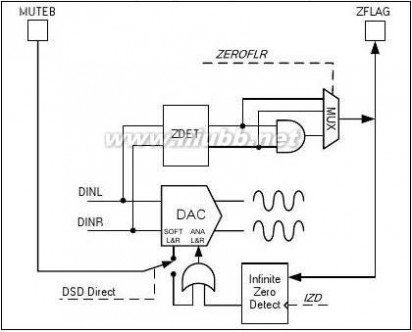
The IZD register configures the operation of the WM8741 analogue mute in conjunction with the zero flag feature. Table 20 shows the interdependency of the MUTEB pin, the IZD register and the zero flag.
REGISTER ADDRESS
R4
Volume Control
04h
BIT
LABEL
DEFAULT
DESCRIPTION
0 = Never analogue mute
1 = Analogue mute when ZFLAG set
Table 20 Infinite Zero Detect Control
w
PP Rev 1.3 October 2007
35
8741 WM8741
WM8741
Product Preview
Figure 25 Software Control Mode MUTEB and ZFLAG Configuration
DE-EMPHASIS
Setting the DEEMPH[1:0] register bits enables de-emphasis support in the WM8741 digital filters. There are three de-emphasis filters, one each for sampling rates of 32kHz, 44.1kHz and 48kHz. REGISTER ADDRESS
R6
Filter Control
06h
Table 34 De-emphasis Control
BIT
LABEL
DEFAULT
00
DESCRIPTION
De-emphasis mode select: 00 = De-emphasis Off 01 = De-emphasis 32kHz 10 = De-emphasis 44.1kHz 11 = De-emphasis 48kHz
[1:0]
OUTPUT PHASE REVERSAL
The REV register bit controls the phase of the output signal. Setting the REV bit causes the phase of the output signal to be inverted. The REV bit can only be used in stereo mode. When in differential mono mode, the REV bit must remain set as 0. REGISTER ADDRESS
R5
Format Control
05h
BIT 6
LABEL REV
DEFAULT
DESCRIPTION
Analogue output phase control: 0 = Normal 1 = Inverted
Table 35 Output Phase Control
w
PP Rev 1.3 October 2007
36
8741 WM8741
Product Preview
WM8741
DIFFERENTIAL MONO MODE
DIFF[1:0] sets the required differential output mode; normal stereo, reversed stereo, mono left or mono right, as shown in Table 36. REGISTER ADDRESS
R8
Mode Control 2
08h
BIT
LABEL
DEFAULT
00
DESCRIPTION
00 = Stereo
10 = Stereo reverse (left and right
channels swapped) 01 = Mono left – differential outputs
VOUTLP (17) is left channel. VOUTLN (16) is left channel inverted.
VOUTRP (12) is left channel inverted.
VOUTRN (13) is left channel. 11 = Mono right – differential outputs.
VOUTLP (17) is right channel inverted.
VOUTLN (16) is right channel. VOUTRP (12) is right channel. VOUTRN (13) is right channel inverted.
Table 36 Differential Output Modes
Using these controls a pair of WM8741 devices may be used to build a dual differential stereo implementation with higher performance and differential output.
DITHER
Dither is applied whenever internal truncation occurs. It is also used when a 32 bit input word is applied to the DAC prior to truncation to the internal wordlength. Three types of dither can be selected to allow the sound quality if the device to be optimised.
TDF has a triangular probability density function and causes zero noise modulation i.e. the quantisation noise is invariant to the changes in the signal level. This mode is recommended and is selected by default.
RPDF has a rectangular probability density function and may cause noise modulation.
HPDF has a triangular probability density function with a high pass characteristic, which has a lower noise at low frequencies at the expense of raised noise levels at higher frequencies. Alternatively the dither can be disabled. REGISTER ADDRESS
R8
Mode Control 2
08h
BIT
LABEL
DEFAULT
10
DESCRIPTION
Digital filter dither mode select: 00 = dither off
01 = RPDF dither applied in Digital filter
10 = TPDF dither applied in Digital filter
11 = HPDF dither applied in Digital filter
Note: DITHER[1:0] applies only to the dither mode in the Digital filter.
[1:0]
Table 37 Dither Control
w
PP Rev 1.3 October 2007
37
8741 WM8741
WM8741
NORMAL PCM MODE DIGITAL FILTER SELECTION
Product Preview
The 8741 has a number of advanced digital filters that can be selected in all PCM operation modes (with the exception of 8FS mode). REGISTER ADDRESS
R6
Filter Control
06h
BIT
LABEL
DEFAULT 000
DESCRIPTION
Selects FIR1 filter response 000 = Response 1 001 = Response 2 010 = Response 3 011 = Response 4 100 = Response 5
Table 38 PCM Advanced Digital Filter Selection
Five digital filters are available for selection in each of the three OSR modes (low, medium and high rate) as selected by the OSR bit described in Table 20. It is recommended that the device is muted before the filter response is changed to prevent noise as the filters are reset from appearing on the outputs.
For full details of the filter characteristics available in normal PCM mode, please see Table 61 to Table 63 and Figure 28 to Figure 57.
8FS MODE DIGITAL FILTER
In 8FS mode, the majority of the internal filters are bypassed. In this mode, the data is filtered using only the filter characteristic described by Table 64 and shown in Figure 58 and Figure 59.
DSD PLUS FILTER SELECTION
The WM8741 has a number of compensation filters that can be selected in DSD Plus mode. REGISTER ADDRESS
R6
Filter Control
06h
BIT
LABEL
DEFAULT
00
DESCRIPTION
Selects Compensation Filter response
00 = Response 1 01 = Response 2 10 = Response 3 11 = Response 4
[1:0]
Table 39 DSD Plus Digital Filter Selection
It is recommended that the device is muted before the filter response is changed to prevent noise as the filters are reset from appearing on the outputs.
Full details of these filters are described in Table 65 and Figure 60 to Figure 67.
DSD DIRECT DIGITAL FILTER
The DSD Direct filter has been designed to provide the minimal of processing to the data with no decimation, re-quantisation or noise-shaping, in order to preserve the signal integrity as much as possible. As a result the filter has a wide bandwidth and a very gradual attenuation. It is recommended that this filter is augmented by analogue post-DAC filtering in order to adhere to the Scarlet-Book SACD standard.
w
PP Rev 1.3 October 2007
38
8741 WM8741
Product Preview
WM8741
DSD MUTE CONTROL
In DSD Direct mode, an analogue mute can be applied at the output of the DAC. This is controlled by register bit AMUTE. REGISTER ADDRESS
R4
Volume Control
04h
BIT
LABEL
DEFAULT
DESCRIPTION
DSD Direct mute control: 0 = mute off 1 = mute on
Table 40 DSD Analogue Mute Control
POWER SAVING STANDBY CONTROL
Setting the PWDN register bit immediately connects all outputs to VMID and resets the digital sections of the DAC system including the DLL, the audio interface and the DSP. Input data samples are not preserved, but all control register settings are maintained. When PWDN is cleared the WM8741 will repeat its power-on initialisation sequence. REGISTER ADDRESS
R5
Format Control
05h
BIT
LABEL
DEFAULT
DESCRIPTION
Power Down Mode Select: 0 = Normal Mode
1 = Power Down Mode
Table 41 Powerdown Control
HARDWARE CONTROL MODE
When the MODE pin is held ‘low’ the WM8741 is set to hardware control mode and a limited feature set can be configured.
24
MODE/ LRSEL
DESCRIPTION
0 = Hardware control mode 1 = 3-wire serial control mode Z = 2-wire serial control mode
Table 42 MODE/LRSEL Hardware Control Pin Function
DSD AND PCM MODE SWITCHING
The audio interface mode can be switched between DSD Direct and PCM by controlling the state of pin DSD. It is recommended that the chip is forced into a MUTE state before dynamically switching modes.
27
SCLK/DSD
DESCRIPTION
0 = PCM Mode
1 = DSD Direct Mode
Table 43 SCLK/DSD Hardware Control Pin Function
AUDIO INPUT FORMAT
Under hardware control, it is possible to select between four different modes of operation for the PCM audio interface. PIN NUMBER STATUS
28 0 0 1
DESCRIPTION
23 0 1 0
16-bit right justified 24-bit right justified 24-bit left justified
I2S
Table 44 CSB/SADDR/I2S and IWO/DOUT Hardware Control Pin Function
w
PP Rev 1.3 October 2007
39
8741 WM8741
WM8741 OVERSAMPLING RATE CONTROL Product Preview
The user has control of the oversampling ratio of the WM8741, and can set to the device to operate in low, medium or high rate modes. For optimum operation of the digital filtering and other processing on the WM8741, the user must ensure the correct value of OSR[1:0] is set at all times. 25 DESCRIPTION OSR/DSDR Oversampling Rate Selection
0 = Low rate (32/44.1/48kHz)
Z = Medium rate (88.2/96kHz)
1 = High rate (176.4/192kHz)
Table 45 OSR/DSDR Hardware Control Pin Function
MUTE PIN
A soft mute can be applied to the WM8741 in the digital domain in all PCM. A logic low on the MUTEB pin will cause the attenuation to ramp to infinite attenuation at a rate of 1022x(4/fs). Setting MUTEB high will return the signal gain to its previous value. Figure 26 shows the soft mute characteristic.
In DSD Direct mode the MUTEB pin controls the analogue mute in the DAC. This analogue mute is a ‘hard’ mute and is applied and released as soon as the MUTEB pin is toggled. 25 MUTEB/
SDOUT DESCRIPTION Mute control 0 = Mute on (no output)
1 = Mute off (normal operation
Table 46 MUTEB Hardware Control Pin Function
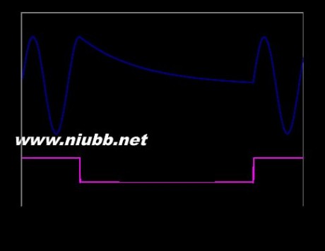
Figure 26 Hardware Control Mode Soft Mute Characteristic
w
PP Rev 1.3 October 2007 40
8741 WM8741
Product Preview WM8741
ZERO FLAG
In hardware control mode the ZFLAG pin asserts when 1024 consecutive zero samples are applied
to the left and right channels of the WM8741 when in PCM mode. In DSD mode, the ZFLAG has no
function.
In hardware mode there is no access to the infinite zero detect and so there is no automute function.
If this functionality is required, software mode must be used. Figure 27 shows the MUTEB and
DE-EMPHASIS CONTROL AND ANTI-CLIPPING MODE
In hardware control mode, de-emphasis is supported at a sampling rate of 44.1kHz. De-emphasis is
supported at 32kHz and 48kHz sampling rates in software control mode.
Audio material is regularly recorded up to 0dB level and heavily compressed. This causes clipping
and distortion when the digital media is applied to a DAC. In order to prevent this in the WM8741, an
anti-clipping mode is provided, which attenuates the digital signal by 2dB as it is processed through
the digital filters.
Under hardware control de-emphasis and the anti-clipping mode are only available when using PCM
mode. 26 SDIN/
DEEMPH DESCRIPTION Deemphasis Control 0 = De-emphasis off
1 = 44.1kHz de-emphasis on
Z = Digital filter anti-clipping mode
Table 47 DEEMPH Hardware Control Pin Function
w
PP Rev 1.3 October 2007 41
8741 WM8741
WM8741
DIGITAL FILTER SELECTION
Product Preview
The WM8741 includes a wide range of digital filters. A limited set of these can be selected in hardware control mode as listed in Table 48. Full details of each digital filter response can be found in section PCM Digital Filter Selection, from page 38.
4
FSEL/ DINR
DESCRIPTION
Digital filter selection (32/44.1/48kHz): 0 = Response 1 1 = Response 4 Z = Response 5
Digital filter selection (88.2/96kHz and 176.4/192kHz): 0 = Response 3 1 = Response 1 Z = Response 2
Table 48 FSEL/DINR Hardware Control Pin Function
There is no choice of digital filters in DSD Direct mode – only the very minimal filtering described in Table 66 is available.
DIFFERENTIAL MONO MODE
If DIFFHW (pin 6) is held to Logic 1, hardware controlled differential mono mode is selected. This overrides any other control pin or register bit. Differential mono mode allows the user to build a dual differential stereo DAC implementation with higher performance and differential output. DIFFHW is used in conjunction with MODE/LRSEL (pin 24) to define a ‘left’ or ‘right’ DAC as shown in Table 49.
PIN NUMBER
6 0
24 0
DESCRIPTION
Hardware control (stereo)
2-wire Software 3-wire software Mono Left – differential outputs VOUTLP = left channel
VOUTLN = left channel inverted VOUTRP = left channel inverted VOUTRN = left channel Mono right – differential outputs VOUTLP = right channel inverted VOUTLN = right channel VOUTRP = right channel
VOUTRN = right channel inverted
Table 49 DIFFHW and MODE/LRSEL Hardware Control Pin Functions
Differential mono mode is available for all PCM hardware controlled modes and DSD Direct hardware mode.
w
PP Rev 1.3 October 2007
42
8741 WM8741
Product Preview
WM8741
OVERVIEW OF FUNCTIONS
The WM8741 has many modes of operation, and certain restrictions on what functions are available in which modes. Table 50 gives an overview of the functions available in hardware and software control modes across all modes of operation:
8FS
PCM MODE Selectable Digital Filters 44.1kHz Deemphasis 32/48kHz Deemphasis Adjustable DSP Dither Differential Mono Mode Digital Softmute Analogue Mute Zero Detect (ZFLAG) Automute Function Anti-Clipping Mode Digital Attenuation Powerdown Mode
Audio Interface Daisy Chain 3-wire Software Interface
Daisy Chain
DSD PLUS
DSD DIRECT
NORMAL PCM
DSD DIRECT
5
9 9 9 9 9 9 9 9 9 9 9 9 9
8 8 8 9 9 9 9 9 8 9 9 9 8 9
4
8 8 9 9 9 9 8 8 8 9 9 8 9
8 8 8 8 9 8 9 8 8 8 8 9 8 9
3
9 8 8 9 9 9 9 8 9 8 8 8 8
8 8 8 8 9 8 9 8 8 8 8 8 8 8
Table 50 Comparison of Functions Available across Operating Modes
9 = function available 8 = function not available
w
PP Rev 1.3 October 2007
43
8741 WM8741
WM8741 REGISTER MAP Reg
0 Name DACLLSB
Attenuation
DACLMSB
Attenuation
DACRLSB
Attenuation
DACRMSB
Attenuation Addr 00h Bit 8 Bit 7 Bit 6 Bit 5 Bit 4 Bit 3 Bit 2 Bit 1 Product Preview Bit 0 Default 0x000 LAT[4:0] 1 01h LAT[9:5] 0x000 2 02h RAT[4:0] 0x000 3 03h RAT[9:5] 0x000 SOFT MUTE 0x000
FMT[1:0] IWL[1:0] 0x00A FIRSEL[2:0] 0x000 OSR[1:0] SR[2:0] MODESEL[1:0] 0x000 0x002 RESET 0x000
w
PP Rev 1.3 October 2007 44
8741 WM8741
Product Preview
REGISTER
ADDRESS
R0
DACLLSB
Attenuation
00h WM8741 DESCRIPTION 00 LSBs of attenuation data for left channel in 0.125dB steps. See Table 25 for details. 0 Attenuation data load control for left channel. 0 = Store LAT[4:0] value but don’t update
1 = Store LAT[4:0] and update attenuation on registers 0-3
Table 51 R0 DACL LSB Attenuation Control Register
REGISTER
ADDRESS
R1
DACLMSB
Attenuation
01h DESCRIPTION 00 MSBs of attenuation data for left channel in 4dB steps. See Table 25 for details. 0 Attenuation data load control for left channel. 0 = Store LAT[9:5] value but don’t update
1 = Store LAT[9:5] and update attenuation on registers 0-3
Table 52 R1 DACL MSB Attenuation Control Register
REGISTER
ADDRESS
R2
DACRLSB
Attenuation
02h DESCRIPTION 00 LSBs of attenuation data for right channel in 0.125dB steps. See Table 25 for details. 0 Attenuation data load control for right channel. 0 = Store RAT[4:0] value but don’t update
1 = Store RAT[4:0] and update attenuation on registers 0-3
Table 53 R2 DACR LSB Attenuation Control Register
REGISTER
ADDRESS
R3
DACRMSB
Attenuation
03h DESCRIPTION 00 MSBs of attenuation data for right channel in 4dB step. See Table 25 for details. 0 Attenuation data load control for right channel. 0 = Store RAT[9:5] value but don’t update
1 = Store RAT[9:5] and update attenuation on registers 0-3
Table 54 R3 DACR MSB Attenuation Control Register
w
PP Rev 1.3 October 2007 45
8741 WM8741
WM8741
REGISTER
ADDRESS
R4
Volume
Control
04h DESCRIPTION 0 Product Preview Ramps volume from existing attenuation setting to new setting when UPDATE applied. 0: Step volume change 1: Ramp volume change
Anti-clipping mode control. Attenuates PCM gain path by 2 dB:
0: 0dB gain
1: -2dB gain 0
Attenuator Control Mode:
0 = Right channels use Right attenuation
1 = Right Channels use Left Attenuation
0 Soft mute select
0: Normal Operation
1: Soft mute both channels 0 = Disable infinite zero detect
1 = Enable infinite zero detect
00 Zero flag output:
00 = Pin assigned to logical AND of LEFT and RIGHT channels
01 = Pin assigned to LEFT channel
10 = Pin assigned to RIGHT channel
11 = ZFLAG disabled [1:0]
0 Applies analogue mute in DSD mode
0 = Normal operation
1 = Analogue mute applied
Table 55 R4 Volume Control Register
REGISTER
ADDRESS
R5
Format
Control
05h DESCRIPTION 10 Audio interface input word length. 00 = 16-bit 01 = 20-bit 10 = 24-bit
11 = 32-bit
Audio data format select.
00 = right justified mode
01 = left justified mode
10 = I2S mode
11 = DSP mode 10
0 = normal LRCLK polarity/DSP mode A
1 = inverted LRCLK polarity/DSP mode B
0 BCLK / DSD64CLK polarity select:
0 = normal polarity
1 = inverted polarity
Analogue output phase control:
0 = Normal
1 = Inverted 5 BCP 6 REV 0
0 Power Down Mode Select:
0 = Normal Mode
1 = Power Down Mode
Table 56 R5 Format Control Register
w
PP Rev 1.3 October 2007 46
8741 WM8741
Product Preview
REGISTER
ADDRESS
R6
Filter Control
06h DESCRIPTION 000 Select advanced digital filter response: 000 = Response 1 001 = Response 2
010 = Response 3
011 = Response 4
100 = Response 5
Select DSD compensation filter response:
00 = Response 1
01 = Response 2
10 = Response 3
11 = Response 4
De-emphasis mode select:
00 = De-emphasis Off
01 = De-emphasis 32kHz
10 = De-emphasis 44.1kHz
11 = De-emphasis 48kHz
ZFLAG Force High Control
0 = Normal operation
1 = Output Logic 1 WM8741 00 [1:0] 00 0
Table 57 R6 Filter Control Register
REGISTER
ADDRESS
R7
Mode Control 1
07h DESCRIPTION [1:0] 00 DSD/PCM mode select. 00 = PCM mode 01 = DSD Direct mode
10 = DSD Plus mode
11 = Unused
000 MCLK to LRCLK sampling rate ratio control:
000 = auto detect sample rate
001 = 128fs
010 = 192fs
011 = 256fs
100 = 384fs
101 = 512fs
110 = 768fs
00 Selects low, medium or high sample rate mode for filter selection
(equivalent to OSR pin functionality in Hardware Mode) 00 = Low rate (32/44.1/48kHz)
01 = Medium rate (96kHz)
10 = High rate (192kHz)
11 = Unused
8FS mode select:
0 = Normal operation
1 = 8FS mode (digital filters bypassed) 0
Table 58 R7 Mode Control Register 1
w
PP Rev 1.3 October 2007 47
8741 WM8741
WM8741 REGISTER
ADDRESS
R8
Mode Control 2
08h DESCRIPTION 10 Product Preview ALU dither mode select: 00 = dither off 01 = RPDF dither applied in ALU
10 = TPDF dither applied in ALU
11 = HPDF dither applied in ALU
Note: DITHER[1:0] applies only to the dither mode in the ALU. 00 = Stereo
10 = Stereo reverse (left and right channels swapped)
01 = Mono left – differential outputs
VOUTLP is left channel.
VOUTLN is left channel inverted.
VOUTRP is left channel inverted.
VOUTRN is left channel.
11 = Mono right – differential outputs.
VOUTLP is right channel inverted.
VOUTLN is right channel.
VOUTRP is right channel.
VOUTRN is right channel inverted. 00
0 Daisychaining Mode. Audio data output control:
0 = No audio data daisychaining
1 = Audio data output on pin 23
0 Daisychaining Mode. Control data output control:
0 = No control data daisychaining
1 = Control data output on pin 25
0 DSD Plus gain control:
0 = Low gain, 1.4Vrms differential output level
1 = High gain, 2.0Vrms differential output level Table 59 R8 Mode Control Register 2
REGISTER
ADDRESS DESCRIPTION
Software reset. Writing to the register resets the entire chip, including R9 the register map. Software reset
09h
Table 60 Software Reset Control Register
w
PP Rev 1.3 October 2007 48
8741 WM8741
Product Preview
WM8741
DIGITAL FILTER CHARACTERISTICS
PCM MODE FILTER CHARACTERISTICS
Low Rate (32/44.1/48kHz) PCM Filter Response 1 Passband Passband Ripple
TYP
-6.02 43 -28.07 8 -6.43 7 -116.19 47 -112.45 8
0.454fs
0.408fs
0.454fs
0.417fs
0.417fs
± 0.000057dB
0.546fs Stopband Attenuation Attenuation at fs/2
-111.8
dB dB fs
Group Delay
Low Rate (32/44.1/48kHz) PCM Filter Response 2 Passband Passband Ripple
± 0.000036 dB
0.522fs Stopband Attenuation Attenuation at fs/2
Fs/2
-111.1
dB dB fs
Group Delay
Low Rate (32/44.1/48kHz) PCM Filter Response 3 Passband Passband Ripple
± 0.000058 dB
0.546fs Stopband Attenuation Attenuation at fs/2
Fs/2
-110.3
dB dB fs
Group Delay
Low Rate (32/44.1/48kHz) PCM Filter Response 4 Passband Passband Ripple
± 0.000066 dB
0.500fs Stopband Attenuation Attenuation at fs/2
Fs/2
-110.4
dB dB fs
Group Delay
Low Rate (32/44.1/48kHz) PCM Filter Response 5 Passband Passband Ripple
± 0.000041 dB
0.500fs Stopband Attenuation Attenuation at fs/2 Group Delay
Fs/2
-111.8
dB dB fs
Table 61 Low Rate PCM Filter Characteristics
w
PP Rev 1.3 October 2007
49
8741 WM8741
WM8741
Medium Rate (88.2/96kHz) PCM Filter Response 1 Passband Passband Ripple
TYP
-120.41 17 -127.96 9 -116.89 48 -126.82 9 -130.52 8
0.208fs
0.208fs
0.417fs
0.208fs
0.208fs
Product Preview
± 0.000021 dB
0.500fs Stopband Attenuation Attenuation at fs/2
Fs/2
-120.3
dB dB fs
Group Delay
Medium Rate (88.2/96kHz) PCM Filter Response 2 Passband Passband Ripple
± 0.000014 dB
0.500fs Stopband Attenuation Attenuation at fs/2
Fs/2
-120.8
dB dB fs
Group Delay
Medium Rate (88.2/96kHz) PCM Filter Response 3 Passband Passband Ripple
± 0.000048 dB
0.500fs Stopband Attenuation Attenuation at fs/2
Fs/2
-115.5
dB dB fs
Group Delay
Medium Rate (88.2/96kHz) PCM Filter Response 4 Passband Passband Ripple
± 0.000021 dB
0.458fs Stopband Attenuation Attenuation at fs/2
Fs/2
-120.0
dB dB fs
Group Delay
Medium Rate (88.2/96kHz) PCM Filter Response 5 Passband Passband Ripple
± 0.000023 dB
0.458fs Stopband Attenuation Attenuation at fs/2 Group Delay
Fs/2
-122.5
dB dB fs
Table 62 Medium Rate PCM Filter Characteristics
w
PP Rev 1.3 October 2007
50
8741 WM8741
Product Preview
High Rate (176.4/192kHz) PCM Filter Response 1 Passband Passband Ripple
TYP
-127.5 10 -124.93 4 -112.67 31 -120.58 6 -128.58 18
0.104fs
0.104fs
0.400fs
0.104fs
0.104fs
WM8741
± 0.000010 dB
0.500fs Stopband Attenuation Attenuation at fs/2
Fs/2
-120.0
dB dB fs
Group Delay
High Rate (176.4/192kHz) PCM Filter Response 2 Passband Passband Ripple
± 0.000031 dB
0.500fs Stopband Attenuation Attenuation at fs/2
Fs/2
-120.0
dB dB fs
Group Delay
High Rate (176.4/192kHz) PCM Filter Response 3 Passband Passband Ripple
± 0.000873 dB
0.500fs Stopband Attenuation Attenuation at fs/2
Fs/2
-110.1
dB dB fs
Group Delay
High Rate (176.4/192kHz) PCM Filter Response 4 Passband Passband Ripple
± 0.000015 dB
0.400fs Stopband Attenuation Attenuation at fs/2
Fs/2
-120.0
dB dB fs
Group Delay
High Rate (176.4/192kHz) PCM Filter Response 5 Passband Passband Ripple
± 0.000001 dB
0.400fs Stopband Attenuation Attenuation at fs/2 Group Delay
Fs/2
-122.8
dB dB fs
Table 63 High Rate PCM Filter Characteristics
8FS MODE FILTER CHARACTERISTICS
8FS Mode Filter Passband Passband Ripple Filter Cut-off Group Delay
TYP
121.13 5
± 0.000021 dB
-3dB point
kHz fs
Table 64 8FS Mode Filter Characteristics
w
PP Rev 1.3 October 2007
51
8741 WM8741
WM8741
DSD PLUS MODE FILTER CHARACTERISTICS
DSD Plus Filter Response 1 Passband Passband Ripple
TYP
58.91 71 49.83 127 49.78 127 49.74 46
Product Preview
± 0.020423 dB
kHz dB kHz fs
127.69 Stopband Attenuation Filter Cut-off
Group Delay
DSD Plus Filter Response 2 Passband Passband Ripple
-3dB point
-38.51
± 0.011308dB
kHz dB kHz fs
120.41 Stopband Attenuation Filter Cut-off
Group Delay
DSD Plus Filter Response 3 Passband Passband Ripple
-3dB point
-44.52
± 0.004140 dB
kHz dB kHz fs
70.03 Stopband Attenuation Filter Cut-off
Group Delay
DSD Plus Filter Response 4 Passband Passband Ripple
-3dB point
-48.05
± 0.019762 dB
kHz dB kHz fs
70.14 Stopband Attenuation Filter Cut-off Group Delay
-3dB point
-26.28
Table 65 DSD Plus Filter Characteristics
DSD DIRECT MODE FILTER CHARACTERISTICS
DSD Direct Filter (Low Gain Mode) Passband Passband Ripple
TYP
83.72 9
± 0.006714 dB
kHz dB kHz fs
116.45 Stopband Attenuation Filter Cut-off Group Delay
-3dB point
-13.82
Table 66 DSD Direct Filter Characteristics
w
PP Rev 1.3 October 2007
52
8741 WM8741
Product Preview
WM8741
PCM MODE FILTER RESPONSES

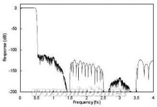
Figure 28 Low Rate PCM Filter 1 Frequency Response
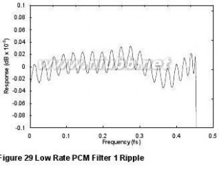
Figure 30 Low Rate PCM Filter 2 Frequency Response
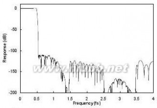
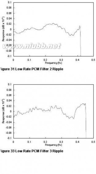
Figure 32 Low Rate PCM Filter 3 Frequency Response
w
PP Rev 1.3 October 2007
53
8741 WM8741
WM8741
Product Preview
Figure 34 Low Rate PCM Filter 4 Frequency Response
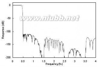
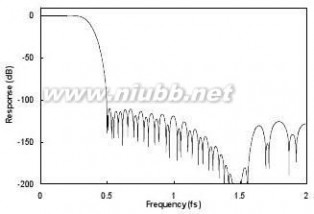
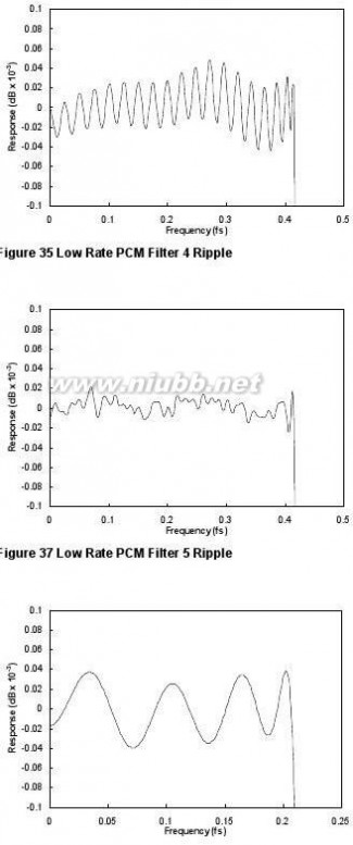
Figure 36 Low Rate PCM Filter 5 Frequency Response
Figure 38 Medium Rate PCM Filter 1 Frequency Response
Figure 39 Medium Rate PCM Filter 1 Ripple
w
PP Rev 1.3 October 2007
54
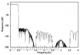
8741 WM8741
Product Preview
WM8741
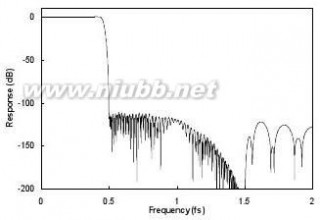
Figure 40 Medium Rate PCM Filter 2 Frequency Response
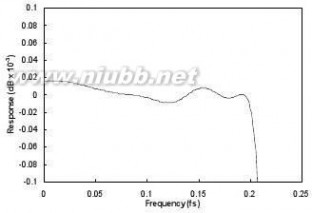
Figure 41 Medium Rate PCM Filter 2 Ripple

Figure 42 Medium Rate PCM Filter 3 Frequency Response

Figure 43 Medium Rate PCM Filter 3 Ripple
Figure 44 Medium Rate PCM Filter 4 Frequency Response
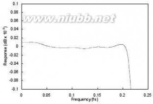
Figure 45 Medium Rate PCM Filter 4 Ripple
w
PP Rev 1.3 October 2007
55
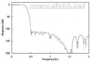
8741 WM8741
WM8741
Product Preview
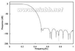
Figure 46 Medium Rate PCM Filter 5 Frequency Response
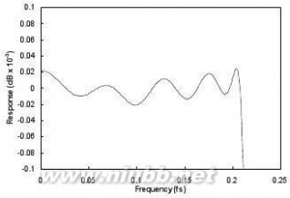
Figure 47 Medium Rate PCM Filter 5 Ripple
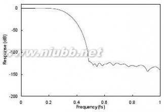
Figure 48 High Rate PCM Filter 1 Frequency Response
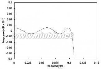
Figure 49 High Rate PCM Filter 1 Ripple
Figure 50 High Rate PCM Filter 2 Frequency Response

Figure 51 High Rate PCM Filter 2 Ripple
w
PP Rev 1.3 October 2007
56
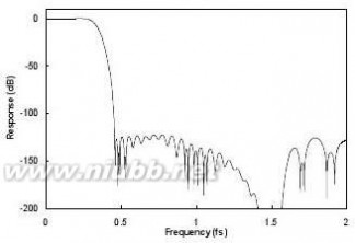
8741 WM8741
Product Preview
WM8741
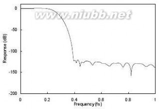
Figure 52 High Rate PCM Filter 3 Frequency Response
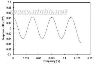
Figure 53 High Rate PCM Filter 3 Ripple
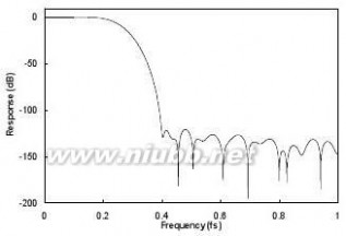
Figure 54 High Rate PCM Filter 4 Frequency Response
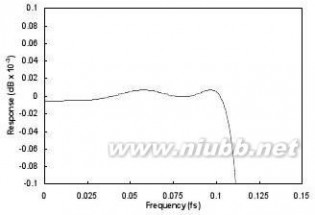
Figure 55 High Rate PCM Filter 4 Ripple
Figure 56 High Rate PCM Filter 5 Frequency Response

Figure 57 High Rate PCM Filter 5 Ripple
w
PP Rev 1.3 October 2007
57

8741 WM8741
WM8741
8FS MODE FILTER RESPONSES
Product Preview
Figure 58 8FS Mode Filter Frequency Response
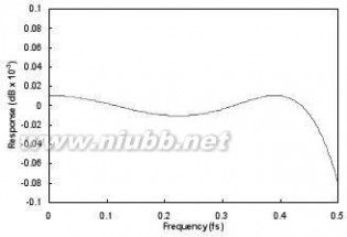
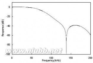
Figure 59 8FS Mode Filter Ripple
DSD PLUS MODE FILTER RESPONSES
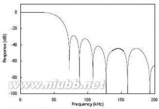
Figure 60 DSD Plus Mode Filter 1 Frequency Response
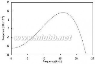
Figure 61 DSD Plus Mode Filter 1 Ripple
Figure 62 DSD Plus Mode Filter 2 Frequency Response
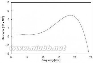
Figure 63 DSD Plus Mode Filter 2 Ripple
w
PP Rev 1.3 October 2007
58
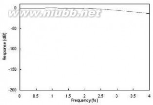
8741 WM8741
Product Preview
WM8741
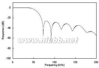
Figure 64 DSD Plus Mode Filter 3 Frequency Response
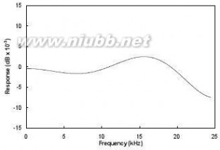
Figure 65 DSD Plus Mode Filter 3 Ripple
Figure 66 DSD Plus Mode Filter 4 Frequency Response


Figure 67 DSD Plus Mode Filter 4 Ripple
DSD DIRECT MODE FILTER RESPONSES
Figure 68 DSD Direct Mode Filter Frequency Response
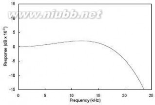
Figure 69 DSD Direct Mode Filter Ripple (Normalised)
w
PP Rev 1.3 October 2007
59
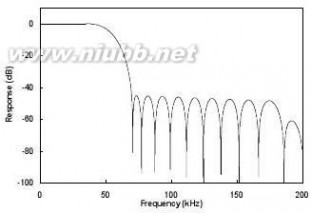
8741 WM8741
WM8741
DEEMPHASIS FILTER RESPONSES
0.0Response (dB)
Response (dB)
-2.0-4.0-6.0-8.0-10.0
5000
10000Frequency (Hz)
Figure 70 De-emphasis frequency response (32kHz)
Product Preview
0.40.30.20.10.0-0.1-0.2-0.3-0.4
5000
10000Frequency (Hz)
15000
20000

1500020000

Figure 71 De-emphasis error (32kHz)
0.0Response (dB)
Response (dB)
5000
10000Frequency (Hz)
Figure 72 De-emphasis frequency response (44.1kHz)
-2.0-4.0-6.0-8.0-10.0
15000
20000

0.40.30.20.10.0-0.1-0.2-0.3-0.4
5000
10000Frequency (Hz)
15000
20000

Figure 73 De-emphasis error (44.1kHz)
0.0
Response (dB)
5000
10000Frequency (Hz)
Figure 74 De-emphasis frequency response (48kHz)
Response (dB)
-2.0-4.0-6.0-8.0-10.0
15000
20000

0.40.30.20.10.0-0.1-0.2-0.3-0.4
5000
10000Frequency (Hz)
15000
20000
Figure 75 De-emphasis error (48kHz)
w
PP Rev 1.3 October 2007
60

8741 WM8741
Product Preview WM8741 APPLICATIONS INFORMATION
Figure 76 External Components

Figure 77 External Filter Components
w
PP Rev 1.3 October 2007 61

8741 WM8741
WM8741 PACKAGE DIMENSIONS
Product Preview Symbols
A
A1
A2
c
e
E
E1
L
L1REF:MIN-----0.051.650.220.099.907.405.000.550Dimensions(mm)NOM----------1.750.30-----10.200.65BSC7.805.300.751.25 REF4MAX2.00.251.850.380.2510.508.205.600.958NOTES:
A. ALL LINEAR DIMENSIONS ARE IN MILLIMETERS.
B. THIS DRAWING IS SUBJECT TO CHANGE WITHOUT NOTICE.
C. BODY DIMENSIONS DO NOT INCLUDE MOLD FLASH OR PROTRUSION, NOT TO EXCEED 0.20MM.
D. MEETS JEDEC.95 MO-150, VARIATION = AH. REFER TO THIS SPECIFICATION FOR FURTHER DETAILS.

w
PP Rev 1.3 October 2007 62
8741 WM8741
Product Preview
WM8741
IMPORTANT NOTICE
Wolfson Microelectronics plc (“Wolfson”) products and services are sold subject to Wolfson’s terms and conditions of sale, delivery and payment supplied at the time of order acknowledgement.
Wolfson warrants performance of its products to the specifications in effect at the date of shipment. Wolfson reserves the right to make changes to its products and specifications or to discontinue any product or service without notice. Customers should therefore obtain the latest version of relevant information from Wolfson to verify that the information is current.
Testing and other quality control techniques are utilised to the extent Wolfson deems necessary to support its warranty. Specific testing of all parameters of each device is not necessarily performed unless required by law or regulation.
In order to minimise risks associated with customer applications, the customer must use adequate design and operating safeguards to minimise inherent or procedural hazards. Wolfson is not liable for applications assistance or customer product design. The customer is solely responsible for its selection and use of Wolfson products. Wolfson is not liable for such selection or use nor for use of any circuitry other than circuitry entirely embodied in a Wolfson product.
Wolfson’s products are not intended for use in life support systems, appliances, nuclear systems or systems where malfunction can reasonably be expected to result in personal injury, death or severe property or environmental damage. Any use of products by the customer for such purposes is at the customer’s own risk.
Wolfson does not grant any licence (express or implied) under any patent right, copyright, mask work right or other intellectual property right of Wolfson covering or relating to any combination, machine, or process in which its products or services might be or are used. Any provision or publication of any third party’s products or services does not constitute Wolfson’s approval, licence, warranty or endorsement thereof. Any third party trade marks contained in this document belong to the respective third party owner.
Reproduction of information from Wolfson datasheets is permissible only if reproduction is without alteration and is accompanied by all associated copyright, proprietary and other notices (including this notice) and conditions. Wolfson is not liable for any unauthorised alteration of such information or for any reliance placed thereon.
Any representations made, warranties given, and/or liabilities accepted by any person which differ from those contained in this datasheet or in Wolfson’s standard terms and conditions of sale, delivery and payment are made, given and/or accepted at that person’s own risk. Wolfson is not liable for any such representations, warranties or liabilities or for any reliance placed thereon by any person.
ADDRESS:
Wolfson Microelectronics plc
Westfield House
26 Westfield Road
Edinburgh
EH11 2QB
Tel :: +44 (0)131 272 7000
Fax :: +44 (0)131 272 7001
Email ::
w
PP Rev 1.3 October 2007 63
本文标题:双wm8741-WM874161阅读| 精彩专题| 最新文章| 热门文章| 苏ICP备13036349号-1